Liquid crystal display and method of manufacturing the same
- Summary
- Abstract
- Description
- Claims
- Application Information
AI Technical Summary
Benefits of technology
Problems solved by technology
Method used
Image
Examples
first embodiment
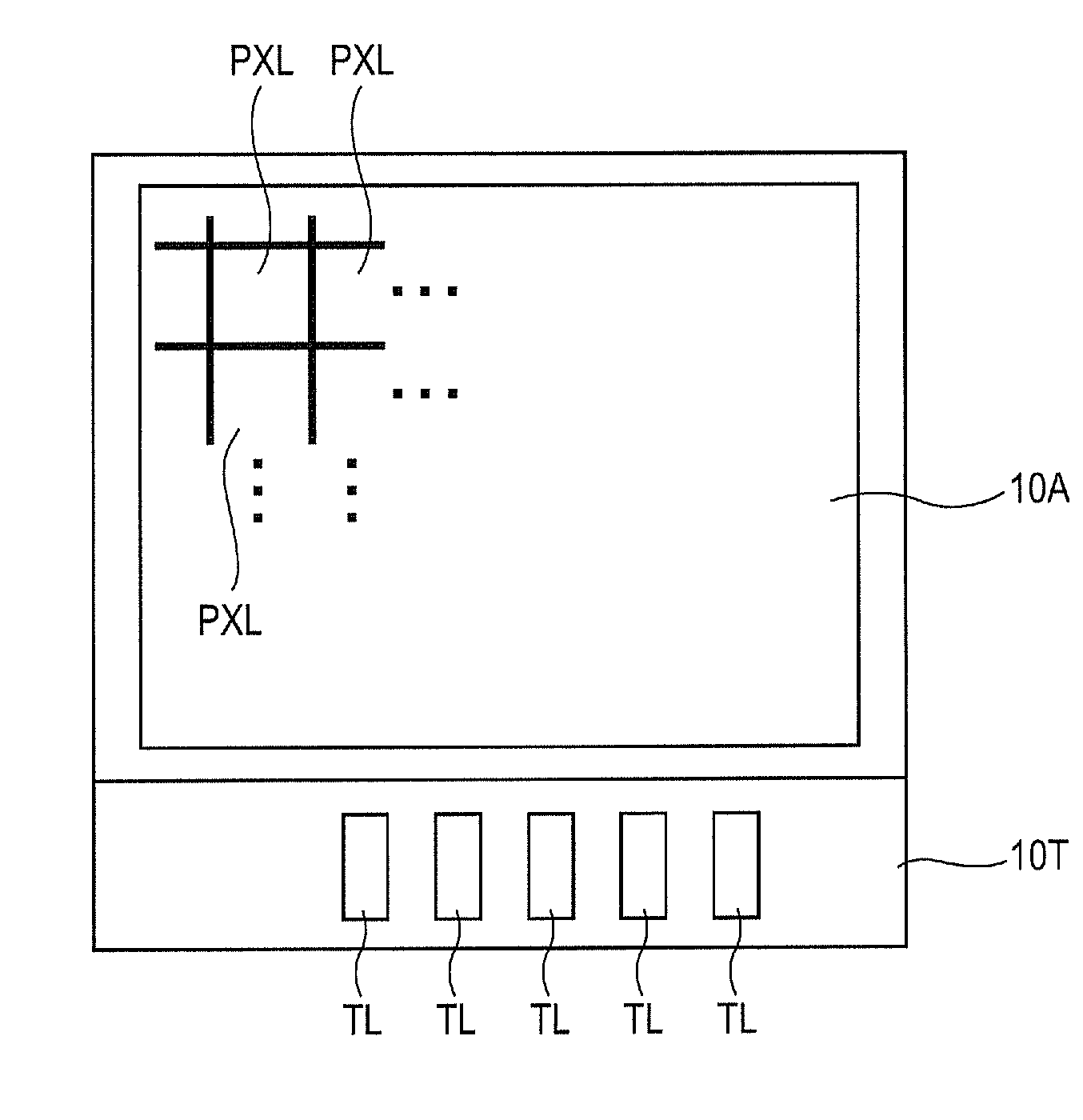
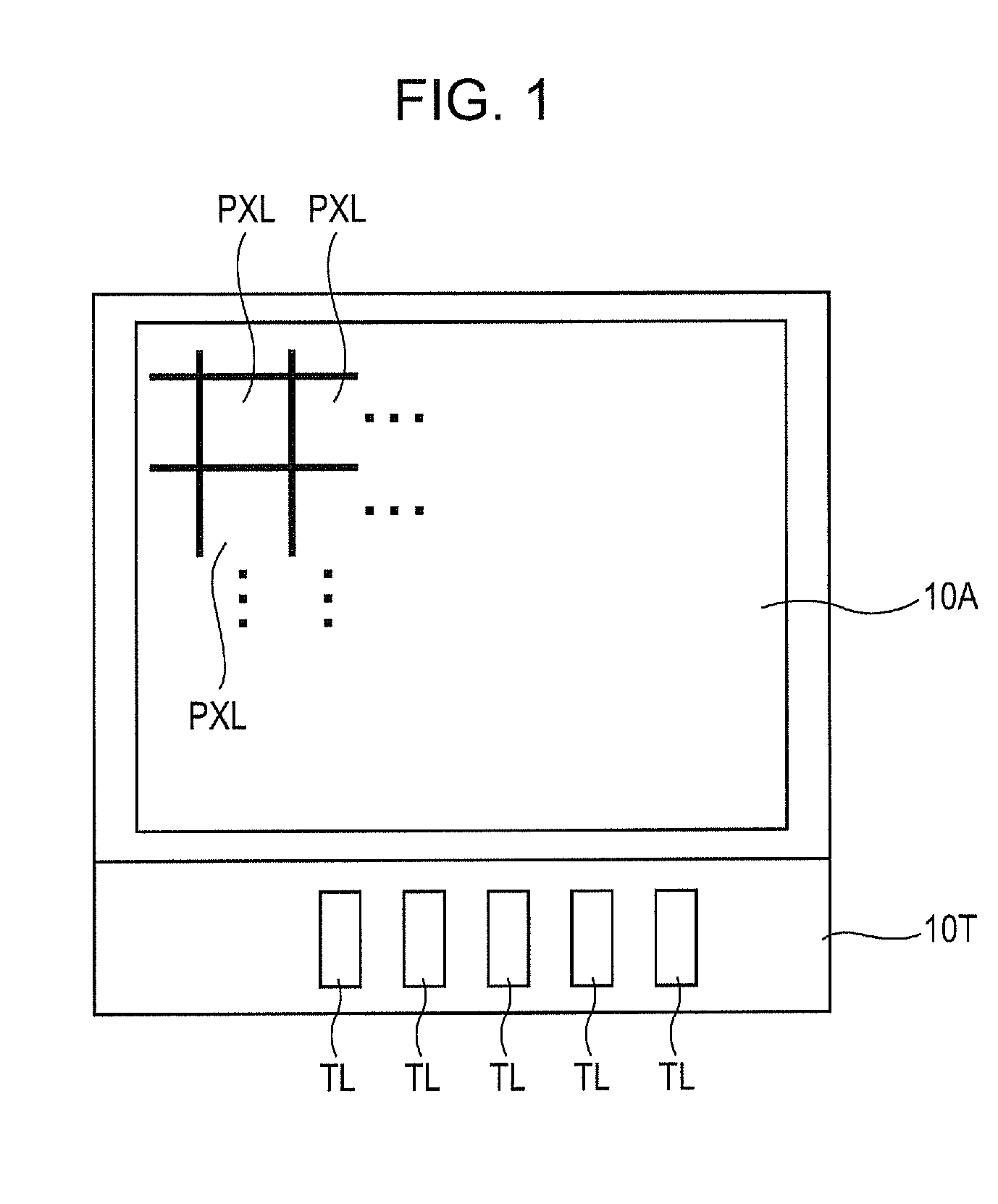
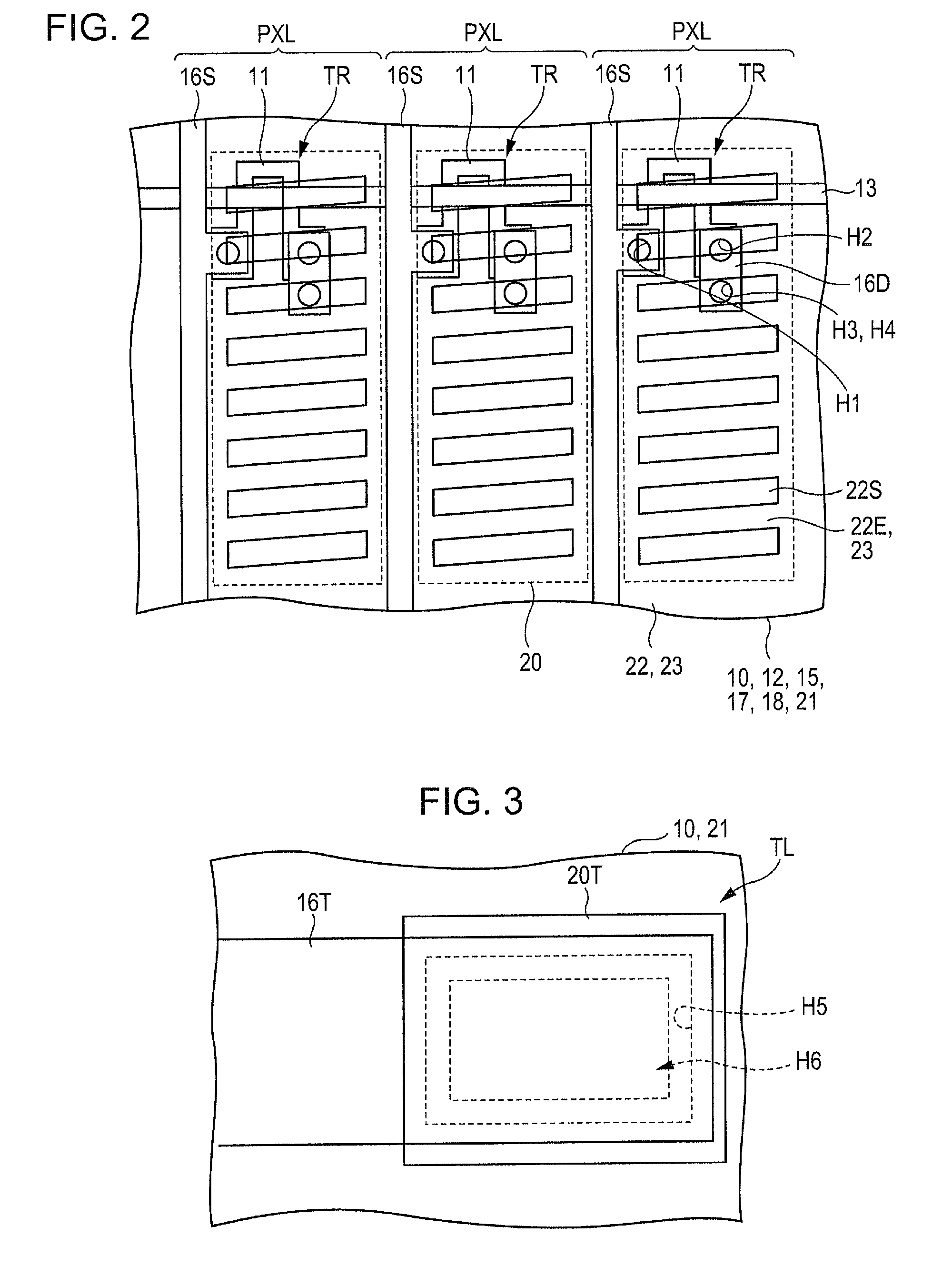
[0056]A liquid crystal display according to a first embodiment of the present invention will now be described with reference to drawings below. FIG. 1 is a schematic plan view of the liquid crystal display. FIG. 2 is an enlarged plan view of three of pixels PXL arranged in a display section 10A, shown in FIG. 1, operating in an FFS mode. FIG. 3 is an enlarged plan view of one of terminals TL arranged in a terminal section 10T shown in FIG. 1. FIGS. 1 to 3 show only principal members of the liquid crystal display for brief description.
[0057]In descriptions below, in order to complement the arrangement of first to fifth contact holes H1 to H5 and openings H6, a gate insulating layer 12, an interlayer insulating layer 15, a passivation layer 17, and a planarization layer 18 are referred to. The correlation between these layers is shown in the description below of a method of manufacturing the liquid crystal display.
[0058]With reference to FIG. 1, the liquid crystal display includes the...
second embodiment
[0064]A second embodiment of the present invention provides a method of manufacturing liquid crystal displays that are the same as the liquid crystal display according to the first embodiment. The method will now be described with reference to drawings below. FIGS. 4A to 7A show one of pixels PXL arranged in a display section 10A included in each liquid crystal display in cross section. FIGS. 4B to 7B show one of terminals TL arranged in a terminal section 10T included in the liquid crystal display in cross section. In FIGS. 4A to 7A and 4B to 7B, the same members as those shown in FIGS. 1 to 3 and 17 are denoted by the same reference numerals as those used in FIGS. 1 to 3 and 17.
[0065]As shown in FIGS. 4A and 4B, active layers 11 are formed in a region of the display section 10A, the region being disposed on a first transparent substrate 10 and being used to form the pixels PXL and pixel transistors TR. A gate insulating layer 12 is formed on the first transparent substrate 10 so a...
third embodiment
[0091]A third embodiment of the present invention provides a method of manufacturing liquid crystal displays. The method will now be described with reference to drawings below. FIGS. 4A, and 9 to 11 show one of pixels PXL arranged in a display section 10A included in each liquid crystal display. In FIGS. 9 to 11, the same members as those shown in FIGS. 1 to 8 and 17 are denoted by the same reference numerals as those used in FIGS. 1 to 8 and 17.
[0092]As shown in FIG. 4A, active layers 11 are formed in a region of the display section 10A, the region being disposed on a first transparent substrate 10 and being used to form the pixels PXL and pixel transistors TR. A gate insulating layer 12 is formed on the first transparent substrate 10 so as to cover the active layers 11. Gate lines 13 are formed on the gate insulating layer 12 so as to overlap the active layers 11. A common electrode line, which is not shown, supplied with a common potential is also formed on a portion of the gate ...
PUM
| Property | Measurement | Unit |
|---|---|---|
| Electrical conductor | aaaaa | aaaaa |
| Transparency | aaaaa | aaaaa |
Abstract
Description
Claims
Application Information


