Inverter Circuit and Method for Operating the Inverter Circuit

a technology of inverter circuit and inverter, which is applied in the direction of dc-ac conversion without reversal, process and machine control, instruments, etc., can solve the problems of increasing switching losses, component costs, and the number of components required

Inactive Publication Date: 2009-10-08
SIEMENS AG
View PDF8 Cites 51 Cited by
  • Summary
  • Abstract
  • Description
  • Claims
  • Application Information

AI Technical Summary

Benefits of technology

[0009]The inverter circuit is suitable for the deployment of small-sized RF transformers, thereby enabling a smaller and less expensive electrically isolated inverter to be implemented. By flexibly designing the primary circuit and disposing only four switches on the secondary side, on the one hand the component costs are minimized and, on the other, the switching losses are limited. Altogether this results in a particularly low-loss, high-efficiency inverter circuit. Moreover, due to the two chokes, the input and output ripple is low and the entire inverter circuit is protected against voltage spikes on both sides.
[0020]An advantageous method provides that, in the event of a positive AC voltage half-cycle and a negative output current, the third switching element is switched in a pulse width modulated manner such that each charging cycle of the transformer begins with the closing of the third switching element and that, in the event of a negative AC voltage half-cycle and a positive output current, the second switching element is switched such that each charging cycle of the transformer begins with the closing of the second switching element. This means that energy can be transferred from the grid to the actual primary side. In addition, this method allows primary-side reactive power absorption and therefore enables the inverter circuit to be used in an island AC voltage grid.

Problems solved by technology

The disadvantage with these topologies, however, is the number of components required, particularly of electronic switches, because this means increased switching losses and component costs.

Method used


Image

  • Inverter Circuit and Method for Operating the Inverter Circuit
  • Inverter Circuit and Method for Operating the Inverter Circuit
  • Inverter Circuit and Method for Operating the Inverter Circuit

Examples


Embodiment Construction

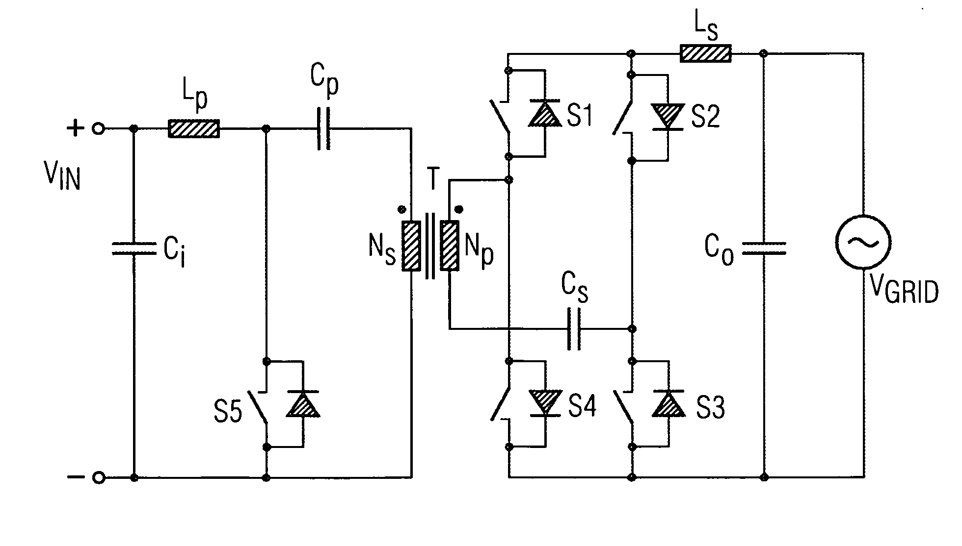
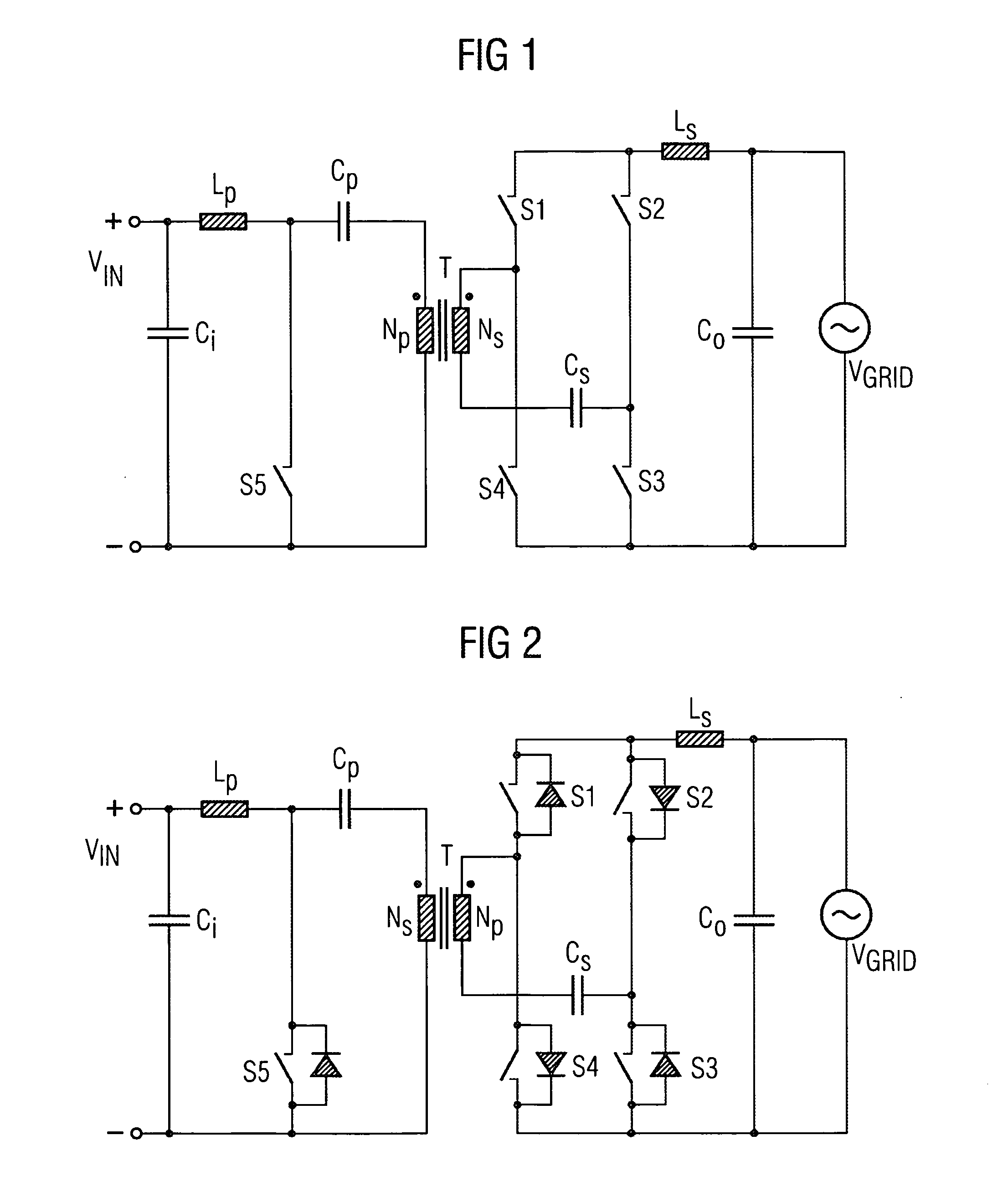
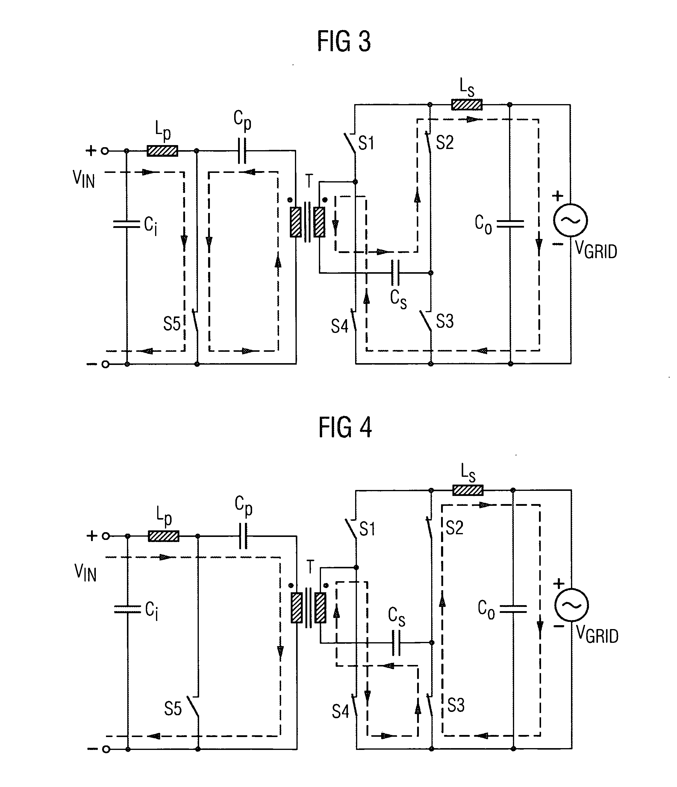
[0057]FIG. 1 shows a primary stage of a Cuk converter comprising a transformer T and a secondary stage implemented as a full bridge. The secondary stage comprises four switching elements S1, S2, S3 and S4 which are interconnected to form a full bridge. The full bridge connects a secondary winding NS disposed on the transformer T in series with a first capacitor CS via a second choke LS and an output capacitor Co to an AC voltage VGRID.

[0058]The primary stage comprises a primary winding NP disposed on the transformer T, said winding being connected in series with a second capacitor CP and a first choke LP via an input capacitor Ci to a DC voltage VIN. Connected in parallel with the primary winding NP and second capacitor CP is a fifth switching element S5.

[0059]The primary and secondary winding NP, NS are disposed on the transformer T with the same winding direction. A three-limb transformer core, for example, can also be used, wherein the primary and secondary windings NP, NS are di...


PUM


Abstract

An inverter circuit having a primary circuit with a first choke for periodically connecting a primary winding to a DC voltage present at an input of the inverter circuit, a secondary circuit with a secondary winding, the secondary winding arranged in series with a first capacitor and connected via a full bridge consisting of four switching elements to a AC voltage present at an output of the inverter circuit via a second choke, and a transformer, wherein the primary circuit and the secondary circuit are electrically isolated by the transformer.

Description

CROSS REFERENCE TO RELATED APPLICATIONS[0001]This application is the US National Stage of International Application No. PCT / EP2007 / 053740 filed Apr. 17, 2007 and claims the benefit thereof. The International Application claims the benefits of German application No. 10 2006 025 975.0 DE filed Jun. 2, 2006. Both of the applications are incorporated by reference herein in their entirety.FIELD OF INVENTION[0002]The invention relates to an inverter circuit comprising a primary circuit and a secondary circuit which are electrically isolated by means of a transformer, wherein the primary circuit comprises means of periodically connecting a primary winding to a DC voltage present at an input of the inverter circuit and wherein the secondary circuit comprises means of connecting a secondary winding to an AC voltage present at an output of the inverter circuit. The invention also relates to methods for operating the inverter circuit.BACKGROUND OF INVENTION[0003]A large number of inverter circ...

Claims


Application Information

Patent Timeline
Patent Type & Authority Applications(United States)
IPC IPC(8): H02M7/5387
CPCH02M3/005H02M7/4807H02M2001/007H02M7/5395H02M7/797H02M7/53806H02M1/007H02M7/48H02M7/521
Inventor HALLAK, JALAL
Owner SIEMENS AG
Why Eureka
Try Eureka