Non-volatile memory with sidewall channels and raised source/drain regions

a non-volatile memory, source/drain region technology, applied in the field of non-volatile memory, can solve the problems of decreasing threshold voltage, increasing device dimensions, and recurring difficulties

Inactive Publication Date: 2009-10-22
SANDISK TECH LLC
View PDF33 Cites 20 Cited by
  • Summary
  • Abstract
  • Description
  • Claims
  • Application Information

AI Technical Summary

Benefits of technology

[0012]In one embodiment, a non-volatile storage system includes non-volatile storage elements formed on a substrate and spaced apart from one another along the substrate in a first direction. Each non-volatile storage element includes an associated bottom insulating layer above the substrate, an associated floating gate above the bottom insulating layer, an associated control gate above the floating gate, and at least one associated sidewall insulating layer extending upwards at least partway along one side of the associated floating gate. Further, epitaxially grown regions extend upwards from the substrate between respective pairs of non-volatile storage elements to a height which is above a bottom level of the floating gates. For each non-volatile storage element, the at least one associated sidewall insulating layer has a thickness near the associated floating gate which is less than about two-thirds of a thickness of the bottom insulating layer.
[0013]In another embodiment, a non-volatile storage system includes non-volatile storage elements formed on a substrate. Each non-volatile storage element includes an associated bottom insulating layer above the substrate, an associated floating gate above the bottom insulating layer, an associated control, and at least one associated sidewall insulating layer extending upwards at least partway along one side of the associated floating gate. Source/drain regions extend upwards from the substrate between respective pairs of non-volatile storage elements to a height which is above a bottom level of the floating gates. For each non-volatile storage element, the at least one associated sidewall insulating layer has a thickn

Problems solved by technology

However, various difficulties arise as device dimensions are scaled ever smaller.
Charge trapping and de-trapping at the tunneling channel can also negatively impact data endurance, resulting in a drop in threshold

Method used


Image

  • Non-volatile memory with sidewall channels and raised source/drain regions
  • Non-volatile memory with sidewall channels and raised source/drain regions
  • Non-volatile memory with sidewall channels and raised source/drain regions

Examples


Embodiment Construction

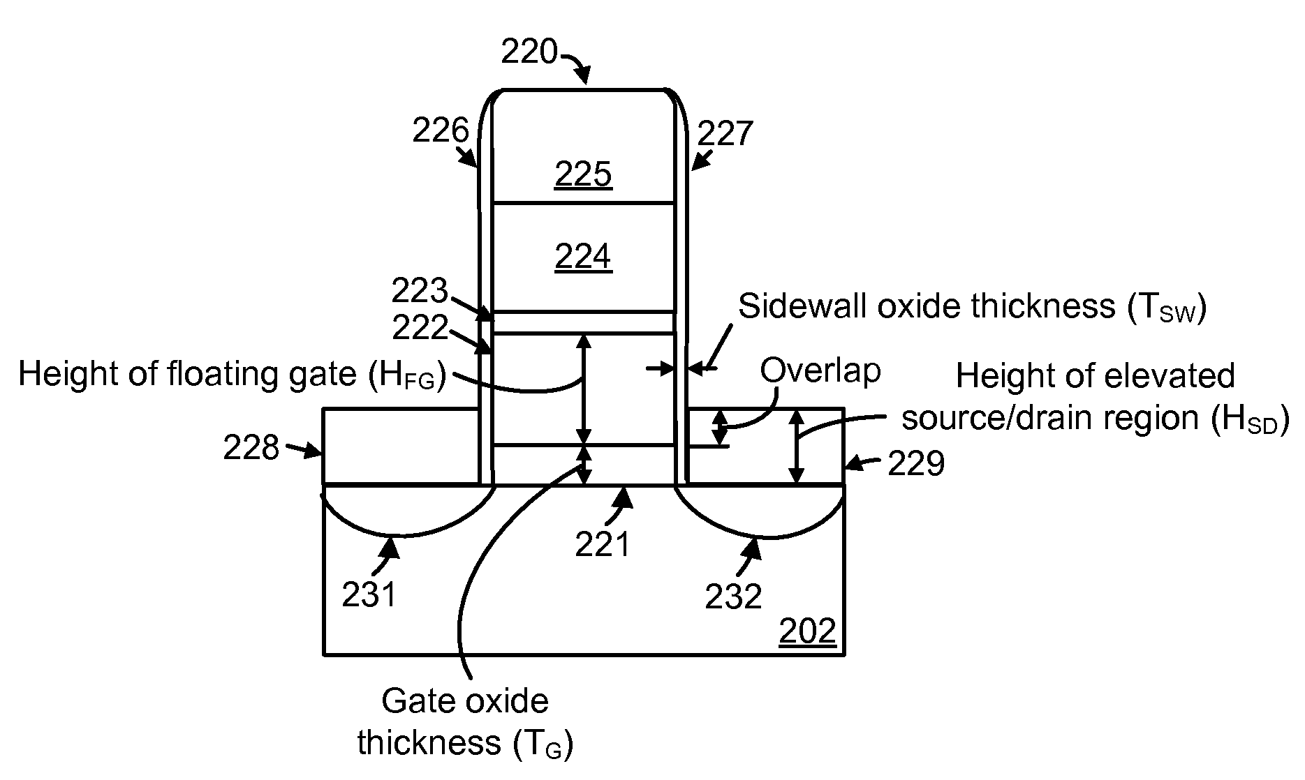
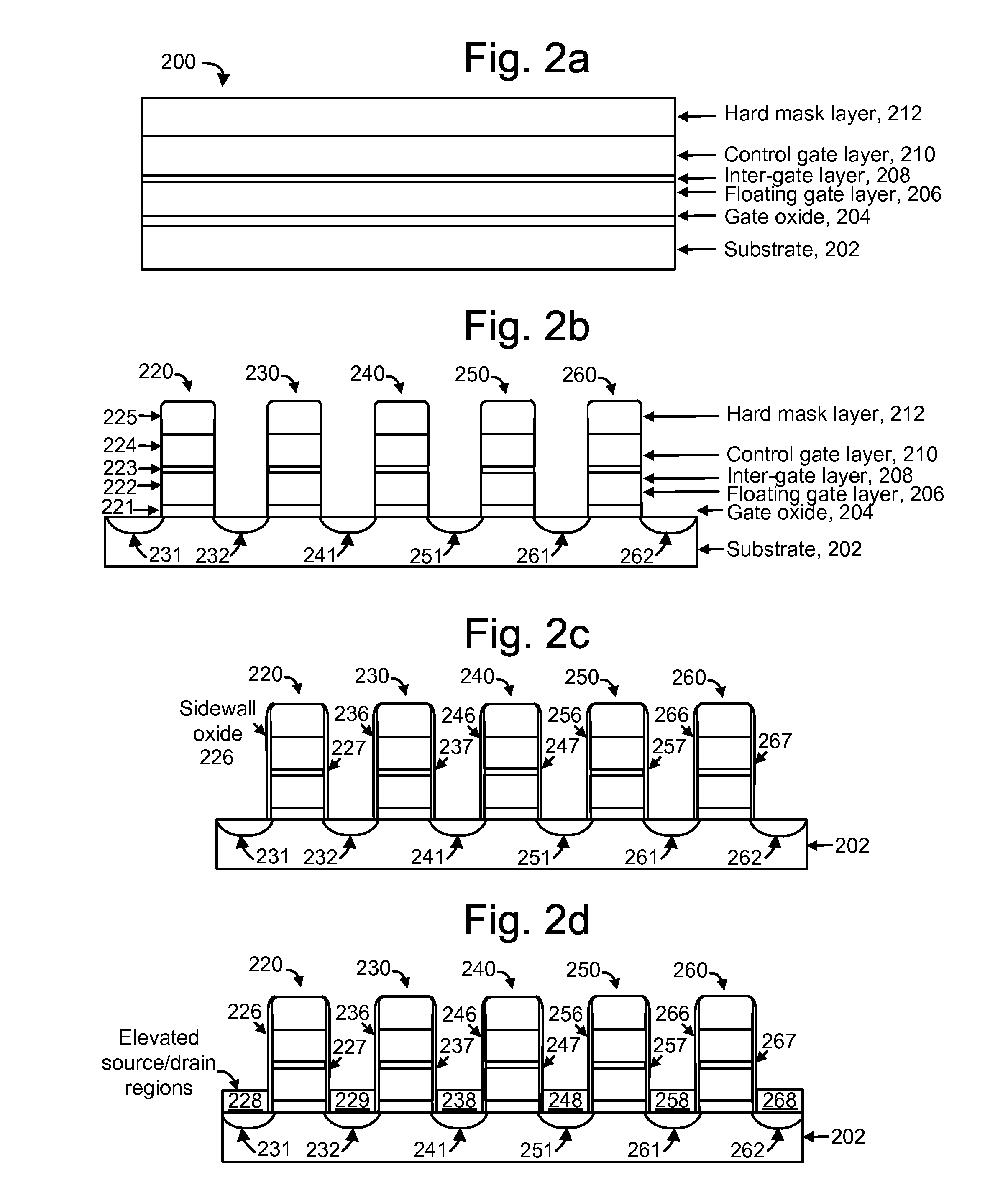
[0049]The present invention provides a non-volatile storage system in which non-volatile storage elements have a reduced sidewall insulating layer thickness relative to a bottom insulating layer thickness to allow sidewall tunneling during programming.

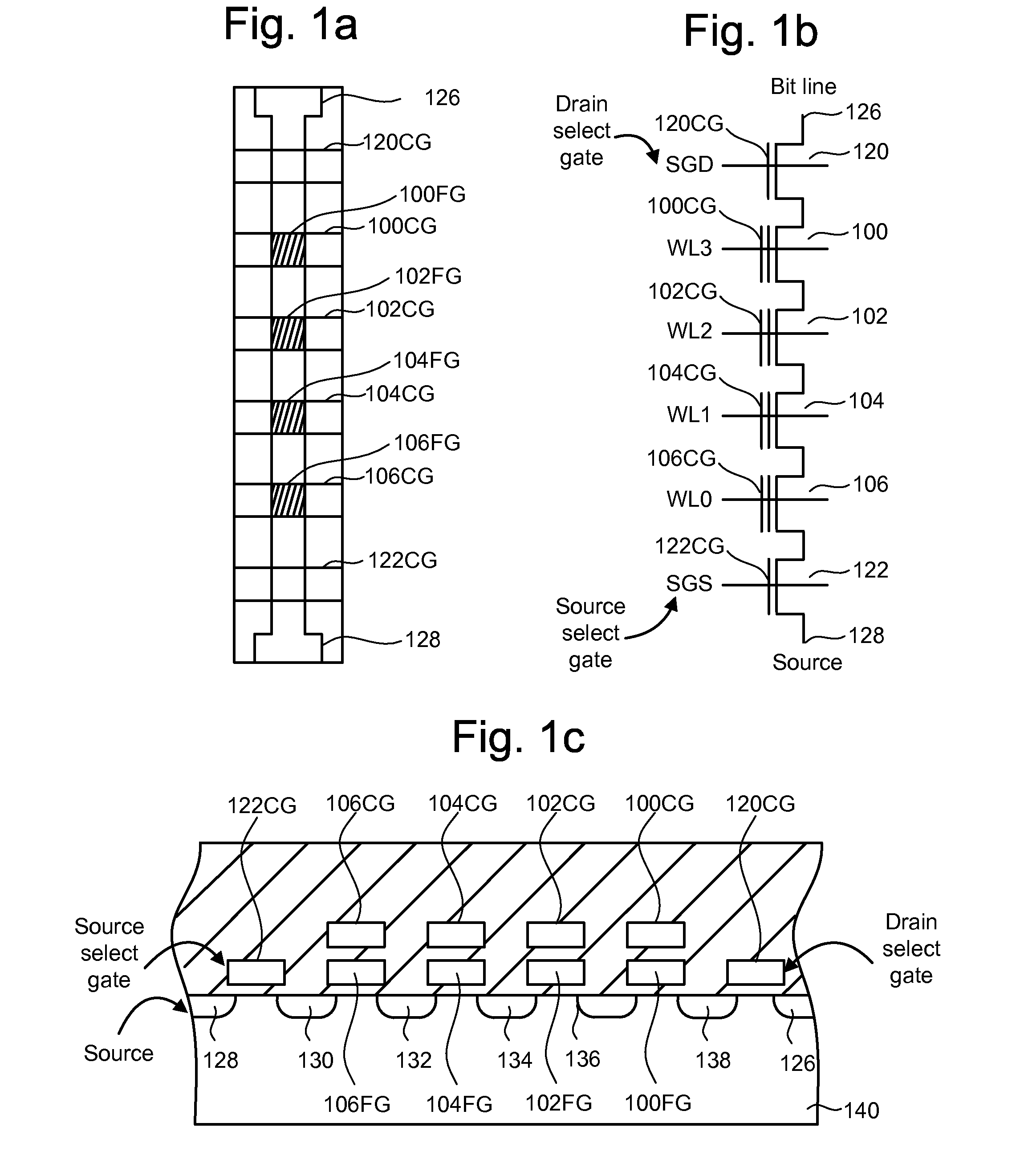
[0050]One example of a non-volatile memory system suitable for implementing the present invention uses the NAND flash memory structure, in which multiple transistors are arranged in series between two select gates in a NAND string. FIG. 1a is a top view showing one NAND string. FIG. 1b is an equivalent circuit thereof. The NAND string depicted in FIGS. 1a and 1b includes four transistors, 100, 102, 104 and 106, in series and sandwiched between a first select gate 120 and a second select gate 122. Select gates 120 and 122 connect the NAND string to bit line contact 126 and source line contact 128, respectively. Select gates 120 and 122 are controlled by applying the appropriate voltages to control gates 120CG and 122CG, respectively. Ea...


PUM


Abstract

A non-volatile storage system in which a sidewall insulating layer of a floating gate is significantly thinner than a thickness of a bottom insulating layer, and in which raised source/drain regions are provided. During programming or erasing, tunneling occurs predominantly via the sidewall insulating layer and the raised source/drain regions instead of via the bottom insulating layer. The floating gate may have a uniform width or an inverted T shape. The raised source/drain regions may be epitaxially grown from the substrate, and may include a doped region above an undoped region so that the channel length is effectively extended from beneath the floating gate and up into the undoped regions, so that short channel effects are reduced. The ratio of the thicknesses of the sidewall insulating layer to the bottom insulating layer may be about 0.3 to 0.67.

Description

BACKGROUND OF THE INVENTION[0001]1. Field of the Invention[0002]The present invention relates to non-volatile memory.[0003]2. Description of the Related Art[0004]Semiconductor memory has become increasingly popular for use in various electronic devices. For example, non-volatile semiconductor memory is used in cellular telephones, digital cameras, personal digital assistants, mobile computing devices, non-mobile computing devices and other devices. Electrically Erasable Programmable Read Only Memory (EEPROM) and flash memory are among the most popular non-volatile semiconductor memories. With flash memory, also a type of EEPROM, the contents of the whole memory array, or of a portion of the memory, can be erased in one step, in contrast to the traditional, full-featured EEPROM.[0005]Both the traditional EEPROM and the flash memory utilize a floating gate that is positioned above and insulated from a channel region in a semiconductor substrate. The floating gate is positioned between...

Claims


Application Information

Patent Timeline
IPC IPC(8): H01L29/788
CPCG11C8/04G11C8/10G11C11/5621H01L27/11521G11C19/00H01L21/28273G11C16/0483H01L29/40114H10B41/30H10B41/35
Inventor CHIEN, HENRYORIMOTO, TAKASHIMATAMIS, GEORGEKAI, JAMESPURAYATH, VINOD R.
Owner SANDISK TECH LLC
Why Eureka
Try Eureka