Microelectromechanical device and method for manufacturing the same

a micro-electromechanical and manufacturing method technology, applied in the direction of micro-structural devices, micro-motors, micro-structured devices, etc., can solve the problem of making the structure of the electronic device b>1/b> more complex, and achieve the effect of convenient and secure manufacturing

Inactive Publication Date: 2009-10-22
KYOCERA CORP
View PDF8 Cites 25 Cited by
  • Summary
  • Abstract
  • Description
  • Claims
  • Application Information

AI Technical Summary

Benefits of technology

[0066]As described above, a plurality of microelectromechanical devices can be easily and securely manufactured. Since the microelectromechanical system remains sealed during separating the electronic component mother substrate and the first mother substrate, cutting dust from the semiconductor substrate such as silicon that arises during separating does not deposit on the microelectromechanical system, and the resulting microelectromechanical system of the microelectromechanical device is less likely to cause malfunction. Thus, microelectromechanical device that operates satisfactorily can be obtained.

Problems solved by technology

This renders the structure of the electronic device 1 more complex, which is a problem.

Method used


Image

  • Microelectromechanical device and method for manufacturing the same
  • Microelectromechanical device and method for manufacturing the same
  • Microelectromechanical device and method for manufacturing the same

Examples


Embodiment Construction

[0081]Preferred embodiments of the present invention will now be described in detail with reference to the drawings.

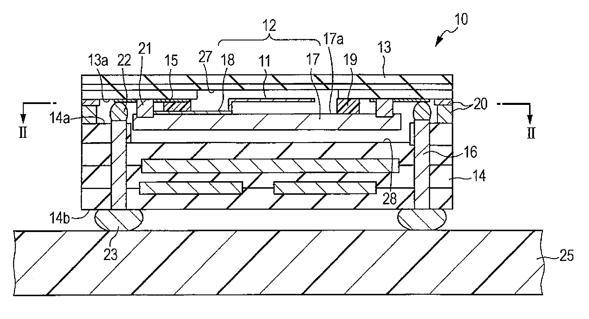
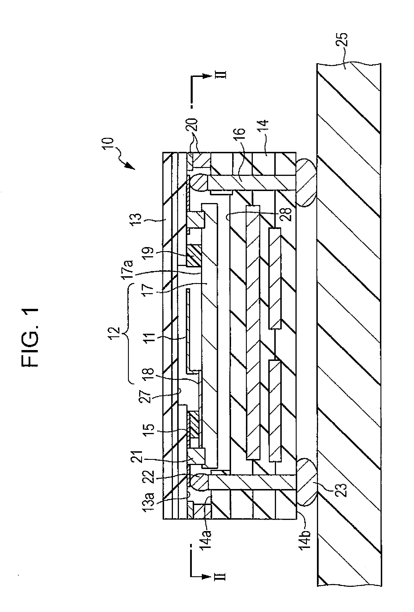
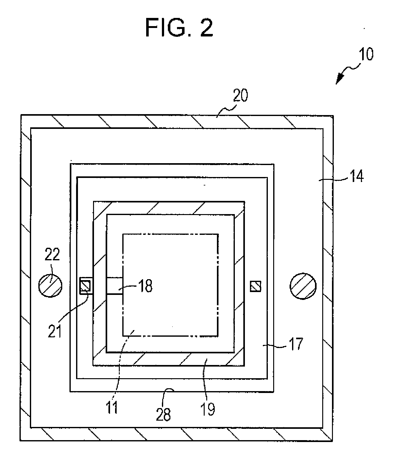
[0082]FIG. 1 is a cross-sectional view of a microelectromechanical device (referred to as “electronic device” hereinafter) 10 according to one embodiment of the present invention. FIG. 2 is a cross-sectional view taken along line II-II in FIG. 1. FIG. 2 shows a cross-section taken along a plane perpendicular to the thickness direction of substrates 13, 14, and 17 described below. Mainly referring to FIG. 1, the electronic device 10 includes a microelectromechanical system (referred to as “MEMS” hereinafter) 11. The MEMS 11 is an electromechanical system constituted by micro components (micro-scale devices) manufactured by making full use of semiconductor fine processing technology. An electronic device 10 including the MEMS 11 is used in a wide variety of field, including sensors such as accelerometers and pressure sensors, optical devices such as micromirror devices w...


PUM


Abstract

The present invention relates to a microelectromechanical device having a simple structure in which strains of the semiconductor substrate can be reduced. Both a semiconductor substrate 17 and a second substrate 14 are disposed to face a first main surface 13a of the first substrate 13 and connected to the first main surface 13a of the first substrate 13. With this structure, no internal line or side surface line is necessary, and the structure of the first substrate 13 can be simplified. The length of the line can be decreased to decrease the resistance of the line, and good electrical characteristics can be achieved at low energy consumption. The strains in the semiconductor substrate 17 can also be reduced.

Description

TECHNICAL FIELD[0001]The present invention relates to a microelectromechanical device including a microelectromechanical system and a method for manufacturing the device.BACKGROUND ART[0002]FIG. 9 is a cross-sectional view of a microelectromechanical device (referred to as “electronic device” hereinafter) 1 of related art. The electronic device 1 is constituted by mounting an electronic component 5, which includes a microelectromechanical system (referred to as “MEMS” hereinafter) 3 and an electrode 4 disposed on a semiconductor substrate 2, onto a first substrate 6 also known as a covering substrate while sealing the MEMS 3. The electronic device 1 can achieve size reduction since the MEMS 3 is sealed with two substrate while being electrically connected to a wire 7 penetrating the first substrate 6 (for example, see Japanese Unexamined Patent Application Publication Nos. 2002-43463 and 2004-296724).[0003]FIG. 10 is a cross-sectional view showing the state in which the electronic d...

Claims


Application Information

Patent Timeline
Patent Type & Authority Applications(United States)
IPC IPC(8): H01L41/053
CPCB81B7/0048B81B2201/0235H01L23/10H01L2924/01079H01L2924/09701H01L2924/1461H01L2224/16H01L2924/00H01L2924/16195
Inventor MAEDA, TOSHIHIKO
Owner KYOCERA CORP
Why Eureka
Try Eureka