Boundary acoustic wave device and method for manufacturing the same
- Summary
- Abstract
- Description
- Claims
- Application Information
AI Technical Summary
Benefits of technology
Problems solved by technology
Method used
Image
Examples
example 1
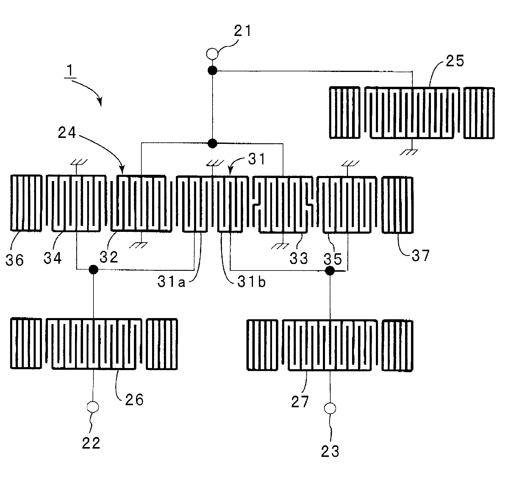
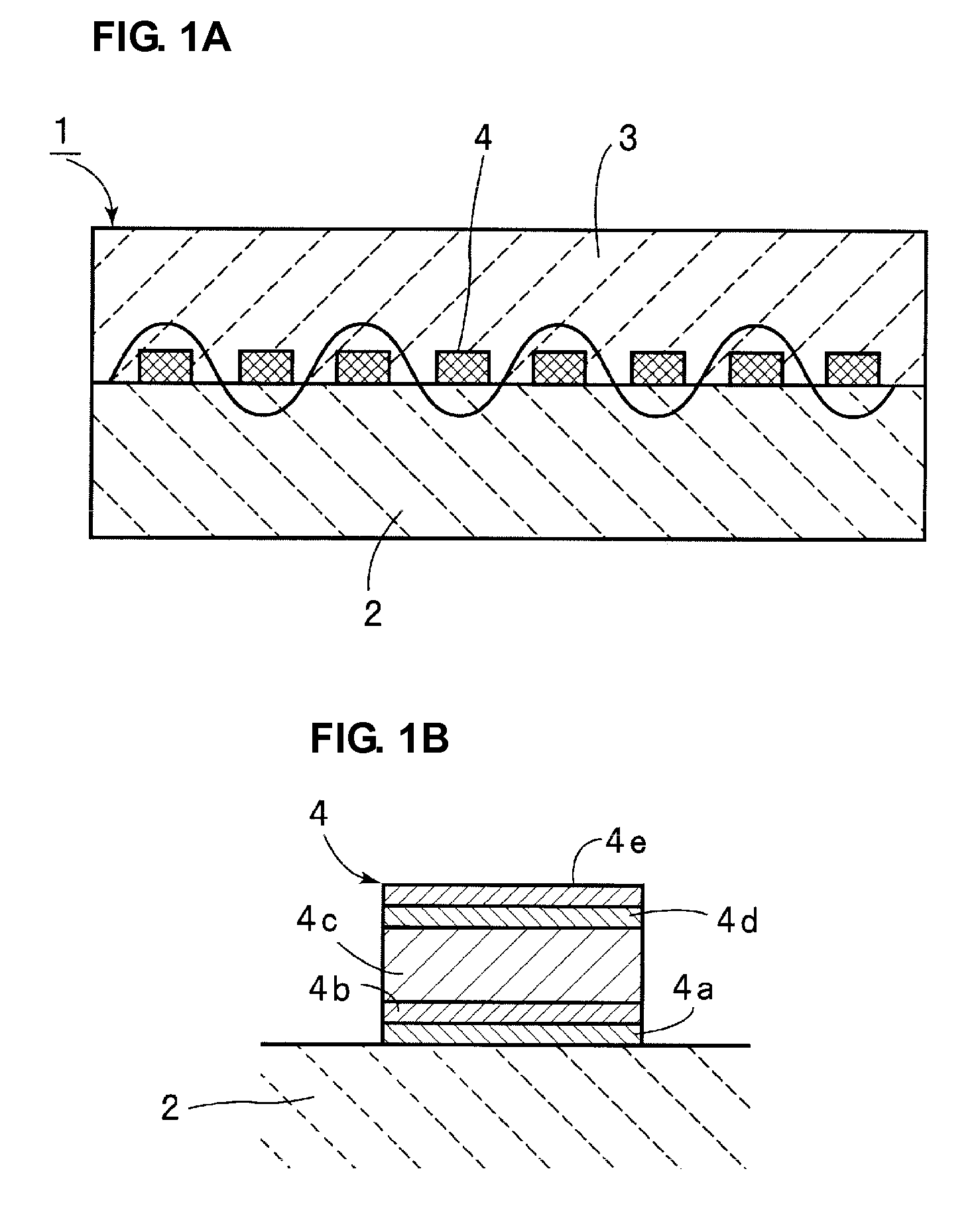
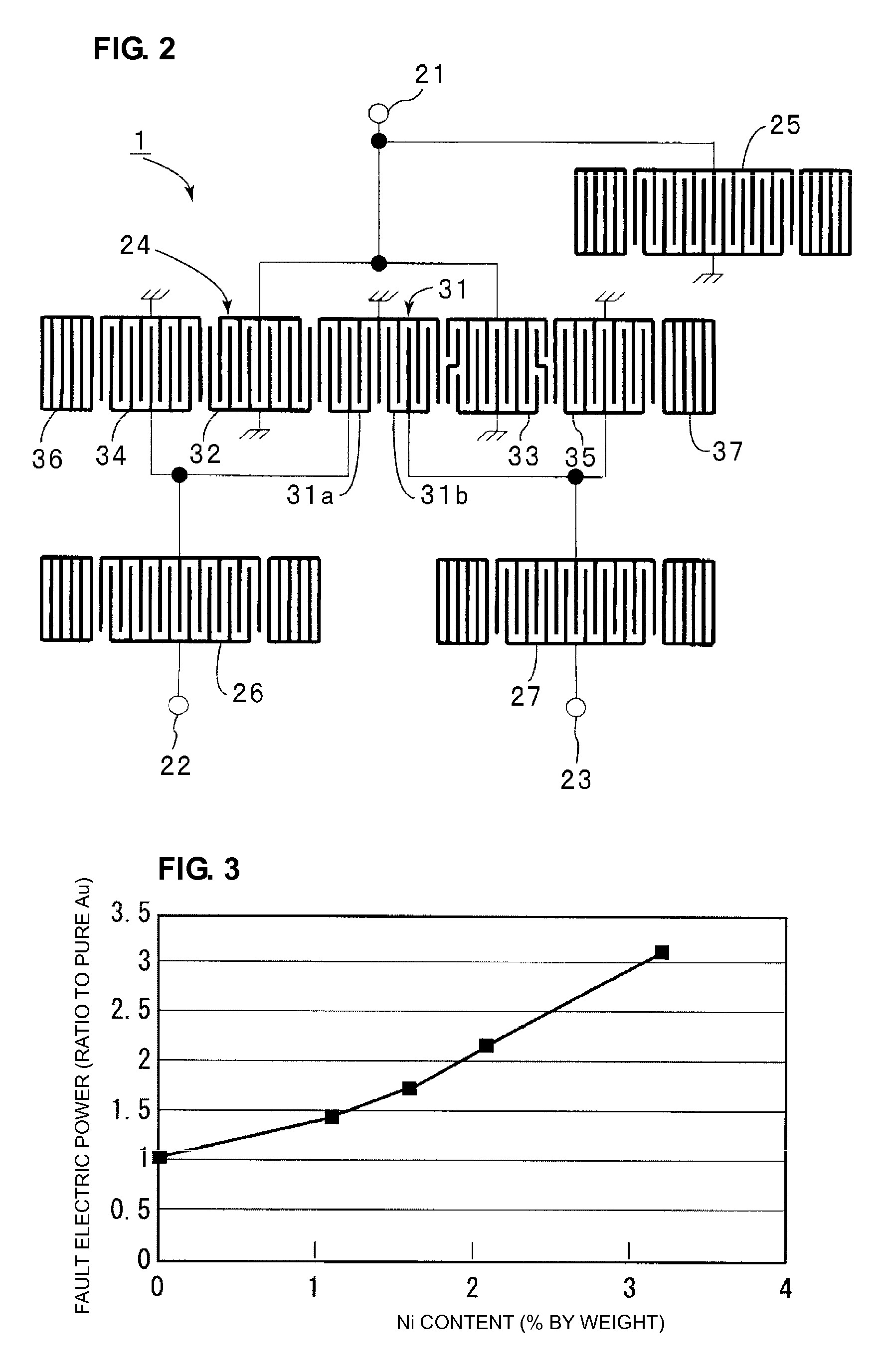
[0036]FIG. 1A is a schematic front sectional view, FIG. 1B is a schematic enlarged front sectional view showing an electrode structure, and FIG. 2 is a plan view showing the electrode structure, for illustrating a boundary acoustic wave filter device according to a preferred embodiment of the present invention.
[0037]A boundary acoustic wave filter device 1 of this preferred embodiment includes a piezoelectric substance 2 and a dielectric substance 3 laminated on the piezoelectric substance 2. As the piezoelectric substance 2, a 15° Y-cut X-propagating LiNbO3 single crystal substrate is preferably used, for example. The dielectric substance 3 is preferably made of SiO2, for example. In addition, an electrode film 4 including an IDT is disposed at the boundary between the piezoelectric substance 2 and the dielectric substance 3, i.e., on the upper surface of the piezoelectric substance 2.
[0038]As the electrode film 4, an IDT and a longitudinally coupled resonator filter portion having...
example 2
[0052]Next, a one-port boundary acoustic wave resonator having an electrode structure shown in FIG. 4A was formed and evaluated. As shown in FIG. 4A, an electrode film 4 is deposited so as to include IDT 11 and reflectors 12 and 13 disposed on both sides of the IDT 11. Although not shown in FIG. 4A, a dielectric substance 3 is laminated to cover the electrode film 4 as in the preferred embodiment shown in FIG. 1A. In this experimental example, a 15° Y-cut X-propagation LiNbO3 single crystal substrate was used as the piezoelectric substance 2. After the electrode film 4 was formed by electron beam evaporation, SiO2 was deposited as the dielectric substance by RF magnetron sputtering.
[0053]As in the electrode film structure shown in FIG. 1B, in the electrode film 4, the IDT 11 was a laminated metal film of Ta film 4a / Pt film 4b / Au alloy film 4c / Pt film 4d / Ti film 4e. The Au alloy film 4c was deposited by electron beam evaporation using an Au alloy including about 1.1% by weight of Cu ...
example 3
[0059]For the boundary acoustic wave filter device 1 evaluated with respect to electric power resistance in Example 1, the Cu content in the Cu-including Au alloy film was changed within the range of about 0.01% to about 4.8% by weight to evaluate the relationship between the insertion loss and the Cu content. The results are shown in Table 2 and FIG. 7.
TABLE 2Cu content (% byweight)Insertion loss (dB)0.011.290.131.250.181.190.51.2111.241.11.281.21.231.71.292.11.333.81.494.81.59
[0060]Table 2 and FIG. 7 show that in an Au alloy film including Cu at a relatively low ratio, the insertion loss is relatively small and improved as compared to the Au alloy film 4c having a Cu content of 0, i.e., pure Au. In particular, at a Cu content within the range of about 0.01% to about 1.7% by weight, the insertion loss is less than that in the pure Au film not including Cu. Therefore, both the electric power resistance and the insertion loss can be improved by using an Au alloy film including Au and...
PUM
| Property | Measurement | Unit |
|---|---|---|
| Fraction | aaaaa | aaaaa |
| Percent by mass | aaaaa | aaaaa |
| Percent by mass | aaaaa | aaaaa |
Abstract
Description
Claims
Application Information


