System and Method of Encapsulation

Active Publication Date: 2009-11-05
QORVO US INC
View PDF46 Cites 115 Cited by
  • Summary
  • Abstract
  • Description
  • Claims
  • Application Information

AI Technical Summary

Benefits of technology

[0012]In another embodiment, a method of encapsulating a device is disclosed. The method includes depositing a first sacrificial layer over the structure, depositing a second sacrificial layer over the first sacrificial layer, and etching the second sacrificial layer and the first sacrificial layer to form a patterned first sacrificial layer and a patterned second sacrificial layer. At least one of the patterned first sacrificial layer and the patterned second sacrificial layer may have a first portion and one or more second portions extending from the first portion. The method may also include depositing a first encapsulating layer over the second sacrificial layer. The first encapsulating layer may be in contact with the structure, the patterned second sacrificial layer and the one or more second portions. The method may additionally include etching the first encapsulating layer to expose a top surface of the one or more second portions and etching the patterned second sacrificial layer and the patterned first sacrificial layer to form a cavity between the first encapsulating layer and the structure and one or more openings through the first encapsulating layer at an area corresponding to the one or more second portions. The method may also include depositing a second encapsulating layer over the first encapsulating layer and the one or more openings to seal the cavity, the second encapsulating layer bordering the cavity.
[0013]In another embodiment, a method of encapsulating a device above a structure is disclosed. The method includes forming one or more electrodes on one or more metal contacts of the structure, depositing a first sacrificial layer over the structure, and depositing a first encapsulating layer over the first sacrificial layer. The first encapsulating layer may have a top surface and sidewalls that extend from the top surface to the structure. The sidewalls may have one or more openings therethrough that expose the first sacrificial layer. Additionally, the first encapsulating layer may be in contact with the one or more electrodes. The method may also include introducing an etchant through the one or more openings, etching the first sacrificial layer to form a cavity between the first encapsulating layer and the structure, and depositing a second encapsulating layer over the first encapsulating layer and the one or more openings to seal the cavity.
[0014]In another embodiment, a method of encapsulating a device above a structure is disclosed. The method may include forming one or more electrodes on one or more metal contacts of the structure, depositing a first sacrificial layer over the structure, and depositing an electrically conductive encapsulating layer over the first sacrificial layer. The electricall

Problems solved by technology

This manufacturing method is complex and time consuming in that several steps are necessary to ensure that the MEMS devices are properly bolted onto the CMOS wafer and properly sealed to protect the MEMS device from the environment.
A problem with these met

Method used


Image

  • System and Method of Encapsulation
  • System and Method of Encapsulation
  • System and Method of Encapsulation

Examples


Embodiment Construction

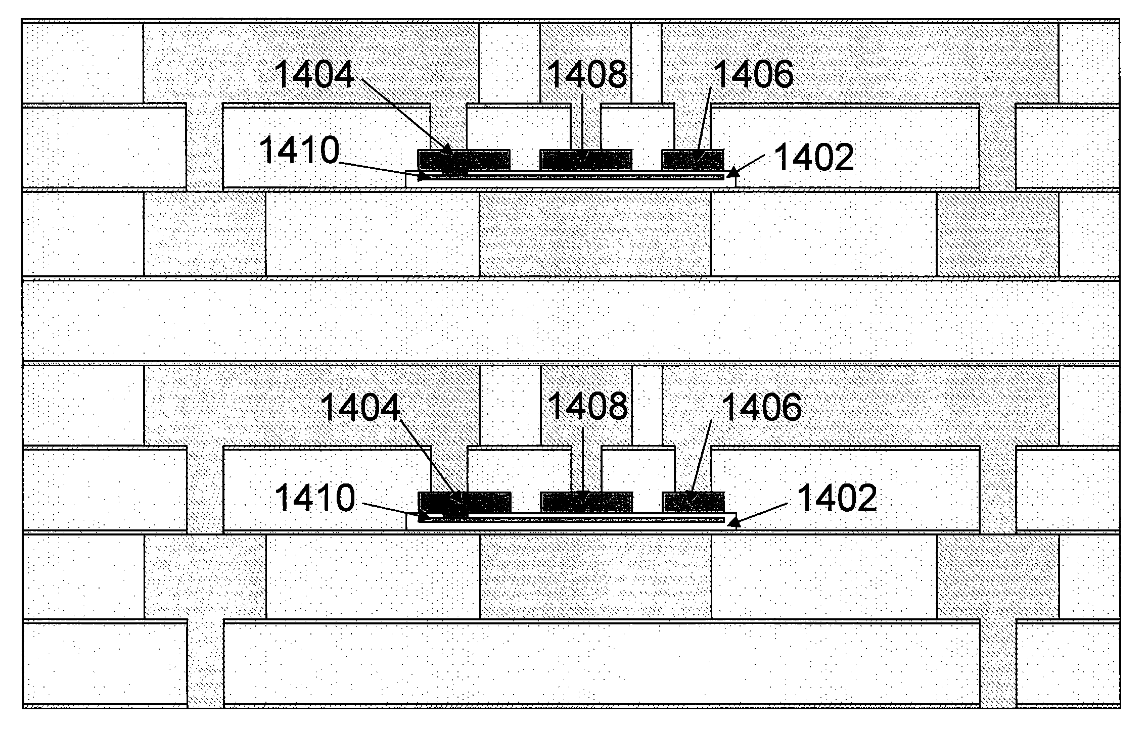
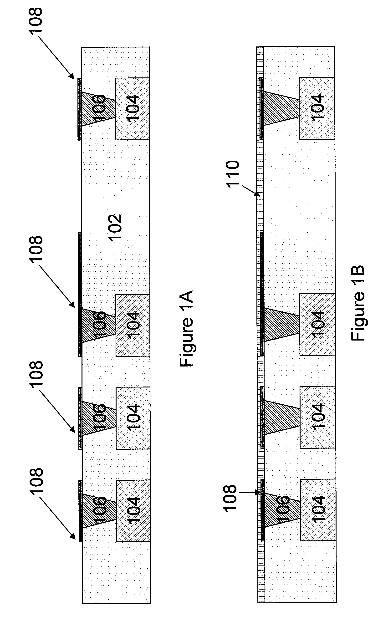
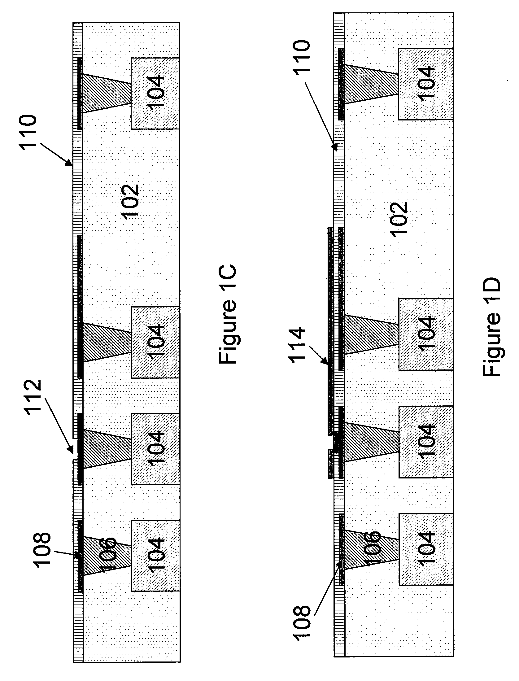
[0036]Embodiments will be described herein with reference to methods of fabricating MEMS devices within a structure. The MEMS device may be formed at any point within the structure. For example, the MEMS device may be formed above a CMOS structure. Additionally, the MEMS device may be formed within a stack such that additional layers of the structure (i.e., not the MEMS device) may be present above the MEMS device. The MEMS device may be used in the BEOL processing of a metal system. In addition it could be formed in the BEOL of a bipolar process or a III / V or II / IV system. The MEMS device may be formed in a cavity above the CMOS BEOL structure, and additional metallization may occur above the MEMS device. The cavity may be formed by depositing an encapsulating layer over the sacrificial layers that enclose the MEMS device. The encapsulating layer may then be etched to expose portions of the sacrificial layers. The sacrificial layers are exposed because they extend through the sidew...


PUM


Abstract

Embodiments discussed herein generally include methods of fabricating MEMS devices within a structure. The MEMS device may be formed in a cavity above the structure, and additional metallization may occur above the MEMS device. The cavity may be formed by depositing an encapsulating layer over the sacrificial layers that enclose the MEMS device. The encapsulating layer may then be etched to expose portions of the sacrificial layers. The sacrificial layers are exposed because they extend through the sidewalls of the encapsulating layer. Therefore, no release holes are etched through the top of the encapsulating layer. An etchant then removes the sacrificial layers to free the MEMS device and form the cavity and an opening through the sidewall of the encapsulating layer. Another encapsulating layer may then be deposited to seal the cavity and the opening.

Description

CROSS-REFERENCE TO RELATED APPLICATIONS[0001]This application claims benefit of U.S. Provisional Patent Application Ser. No. 61 / 126,072, filed Apr. 30, 2008, which is herein incorporated by reference.BACKGROUND OF THE INVENTION[0002]1. Field of the Invention[0003]Embodiments of the present invention generally relate to a method of encapsulating a micro-electromechanical system (MEMS) device, and the device formed thereby.[0004]2. Description of the Related Art[0005]Typical MEMS devices are fabricated as stand alone components which are separately packaged, they can then be coupled with separate microcontroller ships to add functionality. More recently there has been a move to couple these MEMS devices onto a complementary metal-oxide semiconductor (CMOS) by building the MEMS elements on separate wafers and then attaching them to CMOS wafers. This manufacturing method is complex and time consuming in that several steps are necessary to ensure that the MEMS devices are properly bolted...

Claims


Application Information

Patent Timeline
IPC IPC(8): H01L21/56
CPCB81C1/00333B81C2203/0154B81C2203/0145
Inventor LACEY, JOSEPH DAMIAN GORDONRENAULT, MICKAELJOSHI, VIKRAMBOBEY, JAMES F.VAN KAMPEN, ROBERTUS P.
Owner QORVO US INC
Why Eureka
Try Eureka