
Method of Manufacturing a Display Device and Bonding Method

a technology of which is applied in the field of manufacturing a display device and bonding method, can solve the problems of reducing the impact resistan

Inactive Publication Date: 2009-11-19
SEIKO INSTR INC
View PDF3 Cites 162 Cited by
  • Summary
  • Abstract
  • Description
  • Claims
  • Application Information

AI Technical Summary

Benefits of technology

The present invention relates to a method of manufacturing a display device by bonding a polygonal transparent member and a display element together with a transparent adhesive. The method involves applying a liquid transparent adhesive to the bonding surfaces of both members in a dot shape and then linearly connecting the dots. The adhesive is then allowed to drip and fill the gap between the members. The adhesive is then cured using two different curing means, one for the first surface of the transparent member and another for the side surface of the transparent member. The technical effect of this method is to provide a reliable and efficient way to bond polygonal transparent members and display elements together with a transparent adhesive.

Problems solved by technology

Thinning the gap between the perimeter of the flat display and the transparent cover plate into 0.1 mm or less is difficult because it causes problems including the lowering of the impact resistance and the generation of Newton rings.
Air bubbles can also be a problem in the case where an optical adhesive sheet is used to bond the touch panel or the transparent cover plate and the flat display together in full-surface contact.
Bonding by lamination without allowing air bubbles to form is particularly difficult for a thicker and more rigid touch panel or transparent cover plate.
However, with a bonding method disclosed in Patent Document 1, filling the gap with the adhesive uniformly was difficult when the adhesive dripped only on the central part as shown in FIG. 16, and the shortage of the adhesive left the corners unfilled as shown in FIG. 17.

Method used


Image

  • Method of Manufacturing a Display Device and Bonding Method
  • Method of Manufacturing a Display Device and Bonding Method
  • Method of Manufacturing a Display Device and Bonding Method

Examples


embodiment 1

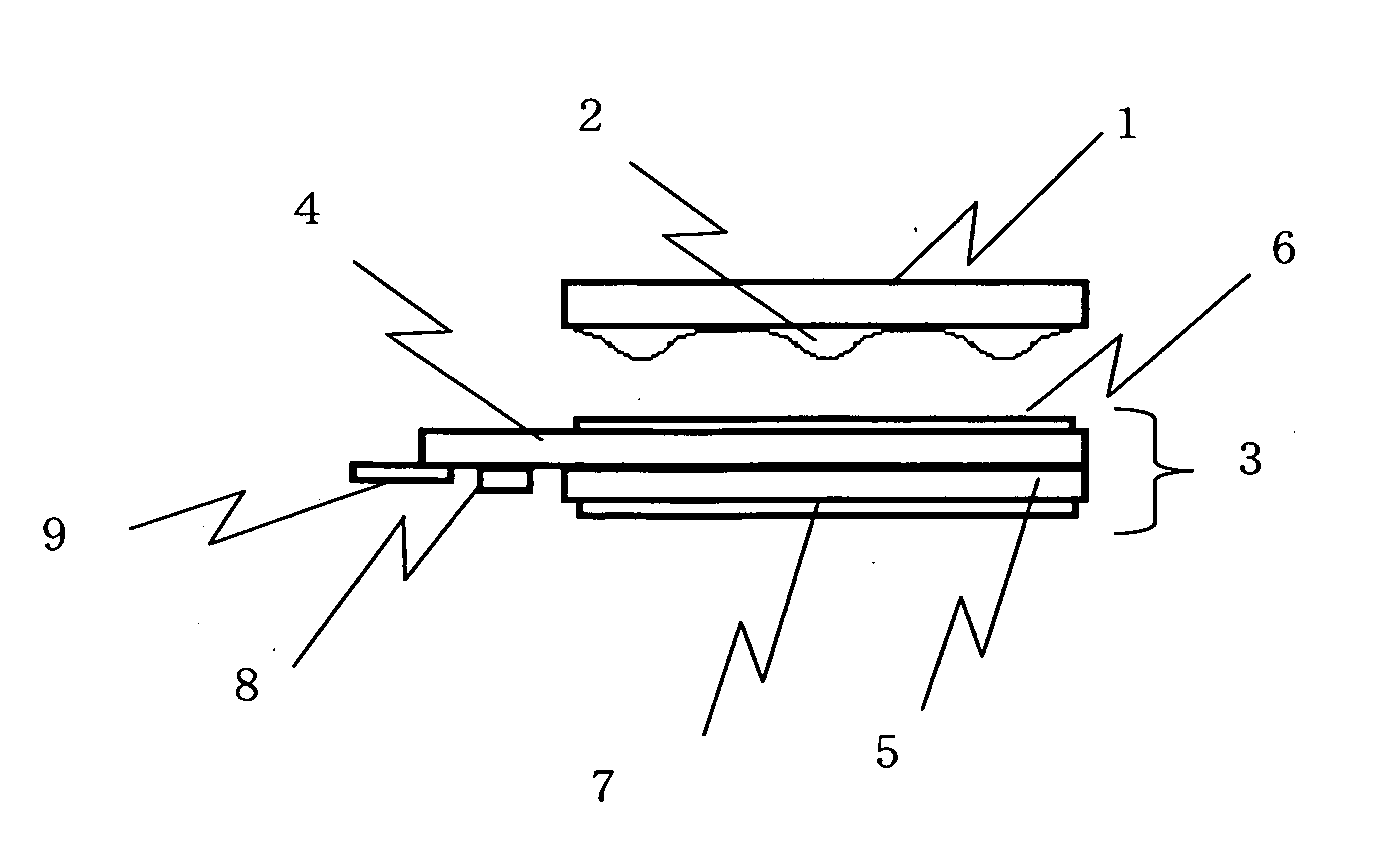
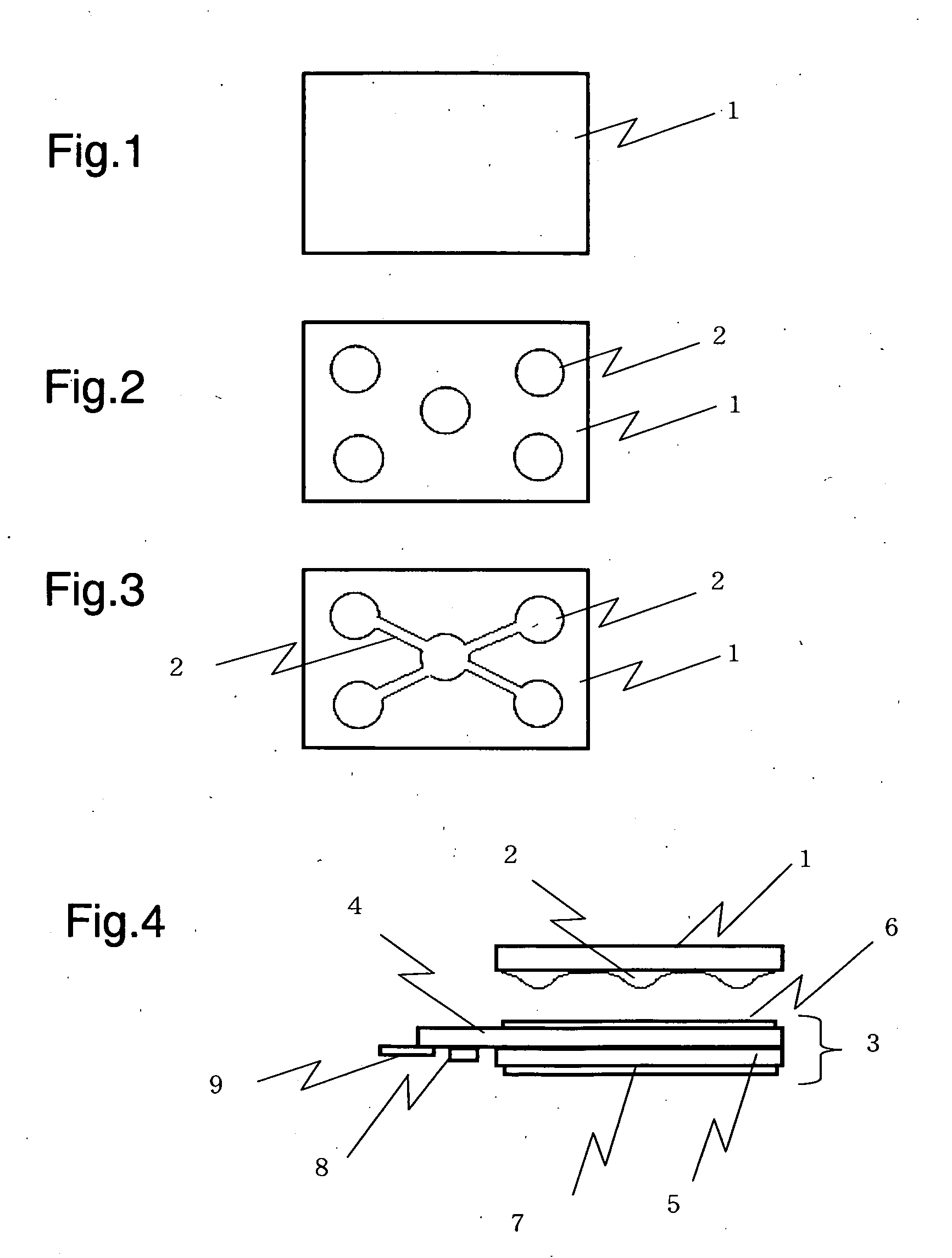
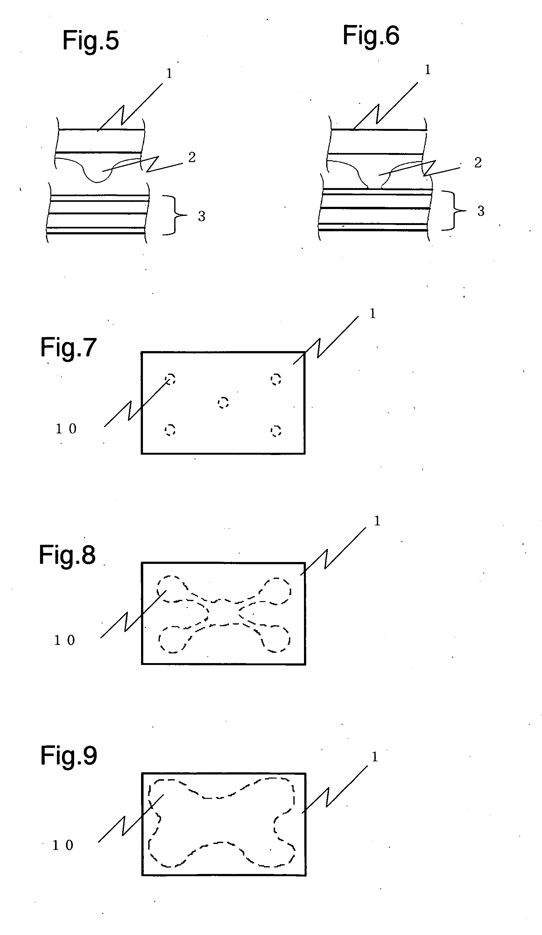
[0039]An embodiment of the present invention is described below with reference to the accompanying drawings. FIG. 1 shows a transparent plate 1, which is placed over the entire front surface of a flat display, and is made from an acrylic material. The transparent plate 1 is 1.5 mm in thickness and 40×40 mm in size. The display is 45×32 mm in external size and 1.3 mm in thickness. The display screen area measures 36×28.5 mm. The display, which is denoted by reference numeral 3, is a liquid crystal display. The display screen of the liquid crystal display 3 is bordered by a frame-shaped, black-colored member, which is formed by printing on the display side. The member formed by printing may be layered on a metal film which is formed by sputtering or the like. FIG. 2 is a top view in which an adhesive 2 is applied to a bonding surface of the transparent plate 1 in dots at the corners and the center, five spots in total. The adhesive 2 applied is about 0.01318 g / cm2 with respect to the ...


PUM

PropertyMeasurementUnit
thicknessaaaaaaaaaa
thicknessaaaaaaaaaa
sizeaaaaaaaaaa

Abstract

Provided is a method of bonding a transparent plate or a touch panel to a flat display without allowing air bubbles to form. A fixed amount of liquid adhesive is applied in dots to a bonding surface around corners and at the center. More adhesive is applied to connect the dots of applied adhesive with lines. The bonding surface is then reversed, causing the adhesive to drip, and the dripping adhesive is brought into contact with an opposite bonding surface to fill a gap between the bonding surfaces with the adhesive. The adhesive is cured by irradiation with light incident from a transparent plate side. In short, after dots of adhesive are brought into contact with the opposite bonding surface and the adhesive flows into a pattern that does not let in air bubbles, the gap between the bonding surfaces is filled with the adhesive.

Description

BACKGROUND OF THE INVENTION[0001]1. Field of the Invention[0002]The present invention relates to a method of bonding a transparent substrate and a substrate together with a liquid adhesive in a manner that brings the two into full-surface contact with each other. For example, the present invention relates to bonding a transparent cover plate of a cellular phone or other similar devices to a flat display such as a liquid crystal display device, a plasma display, an organic EL display, an inorganic EL display, or an FED, or bonding a touch panel to a flat display.[0003]2. Description of the Related Art[0004]A known method to place a transparent touch panel on a display panel is to fix the transparent touch panel to the perimeter of the display panel by adhesion provided by double-sided adhesive tape between 0.3 to 0.5 mm and 1 mm in thickness, or thicker. Another known method is to bond the display panel and the touch panel together in full-surface contact with the use of an optical a...

Claims


Application Information

Patent Timeline
Patent Type & Authority Applications(United States)
IPC IPC(8): B32B37/12
CPCB29C65/1406B29C66/91645B29C65/1435B29C65/4845B29C65/52B29C65/782B29C66/21B29C66/342B29C66/45B29K2709/08B29K2995/0026B29L2031/3475B32B37/003B32B37/1284B32B37/1292B32B2457/20B32B2457/206C09J5/00G02F1/133308G02F2001/133311G02F2202/28B29C65/1409B29C66/73366B29C65/1483B29C65/1448B29C65/00B29C66/1122B29C66/71B29C66/8322G02F1/133311B29K2033/12B29K2069/00G02F1/1333G09F9/00
Inventor MATSUHIRA, TSUTOMU
Owner SEIKO INSTR INC
Learn More