Memory devices with selective pre-write verification and methods of operation thereof

Active Publication Date: 2009-11-19
SAMSUNG ELECTRONICS CO LTD
View PDF5 Cites 30 Cited by
  • Summary
  • Abstract
  • Description
  • Claims
  • Application Information

AI Technical Summary

Benefits of technology

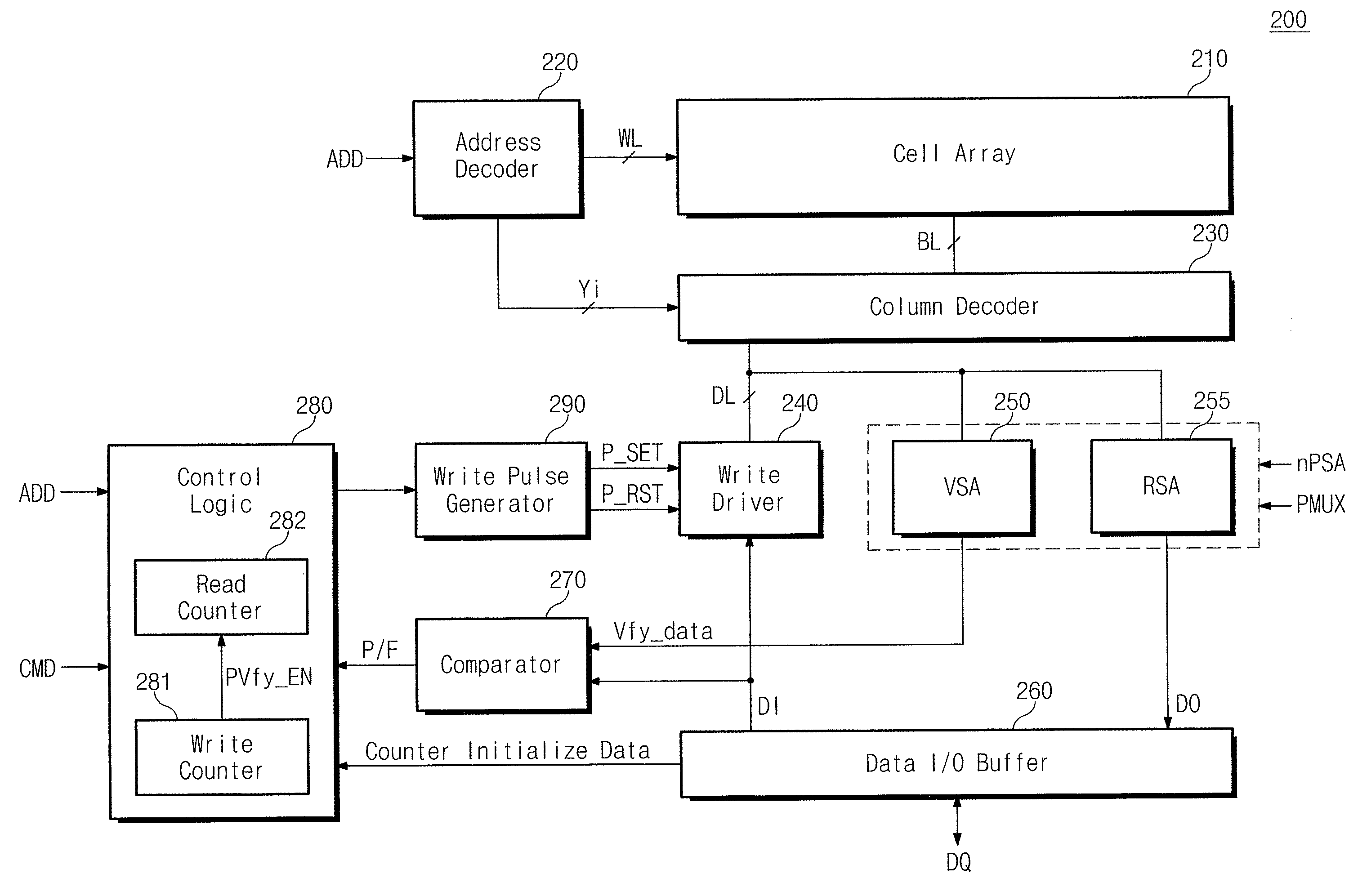
[0016]Further embodiments of the present invention provide a memory device including a memory comprising a plurality of memory locations. The memory device further includes a control circuit configured to monitor a number of read cycles applied to a selected memory location of the plurality of memory locations and to selectively pre-write verify and write received write data to the selected memory location based on the monitored number of read cycles. The control circuit may be configured to enable and inhibit pre-write verification responsive to a pre-write verify enable signal. The control circuit may further include a write counter configured to count write cycles applied to the memory and to control the pre-write verify enable signal responsive to the count of write cycles. The control circuit may be configured to monitor a number of successive read operations occurring without writing to the selected memory location and to selectively pre-write verify and write received write data to the selected memory location based on the monitored number of successive read cycles. The control circuit may be configured to maintain a c

Problems solved by technology

One of issues that may be raised when realizing a phas

Method used


Image

  • Memory devices with selective pre-write verification and methods of operation thereof
  • Memory devices with selective pre-write verification and methods of operation thereof
  • Memory devices with selective pre-write verification and methods of operation thereof

Examples


Embodiment Construction

[0028]Embodiments of the present invention will now be described hereinafter with reference to the accompanying drawings. However, this invention should not be construed as limited to the embodiments set forth herein. Rather, these embodiments are provided so that this disclosure will be thorough and complete, and will fully convey the scope of the invention to those skilled in the art. Like numbers refer to like elements throughout. As used herein the term “and / or” includes any and all combinations of one or more of the associated listed items and may be abbreviated as “ / ”.

[0029]The terminology used herein is for the purpose of describing particular embodiments only and is not intended to be limiting of the invention. As used herein, the singular forms “a,”“an” and “the” are intended to include the plural forms as well, unless the context clearly indicates otherwise. It will be further understood that the terms “comprises,”“comprising,”“having,”“having,”“includes,”“including” and / o...


PUM


Abstract

A number of read cycles applied to a selected memory location of a memory device, such as a variable-resistance memory device, is monitored. Write data to be written to the selected memory location is received. Selective pre-write verifying and writing of the received write data to the selected memory location occurs based on the monitored number of read cycles. Selectively pre-write verifying and writing of the received write data may include, for example, writing received write data to the selected memory cell region without pre-write verification responsive to the monitored number of read cycles being greater than a predetermined number of read cycles

Description

CROSS-REFERENCE TO RELATE APPLICATIONS[0001]This application claims priority under 35 U.S.C §119 to Korean Patent Application No. 10-2008-0046134, filed on May 19, 2008, in the Korean Intellectual Property Office, the entire contents of which are incorporated by reference.BACKGROUND[0002]1. Technical Field[0003]The present invention relates to semiconductor memory devices and, more particularly, to memory devices and methods of operation thereof.[0004]2. Description of Related Art[0005]There is an increasing demand for semiconductor memory devices capable of random access, high integration and large capacity. Such semiconductor memory devices include flash memory devices, which are used, for example, in portable electronic devices. Semiconductor memory devices which substitute non-volatile material for capacitors in DRAM-like structures have also been introduced. Such devices include, for example, ferroelectric RAM (RFAM) devices that use ferroelectric capacitors, magnetic RAM (MRAM...

Claims


Application Information

Patent Timeline
IPC IPC(8): G11C11/00G11C7/00
CPCG11C7/1006G11C8/10G11C13/0004G11C2013/0076G11C13/0069G11C16/3459G11C13/0064G11C13/0035G11C7/22G11C13/02
Inventor JEONG, HONG-SIKLEE, KWANG-JINHA, DAE-WONJEONG, GI-TAELEE, JUNG-HYUK
Owner SAMSUNG ELECTRONICS CO LTD
Why Eureka
Try Eureka