Supercharge Your Innovation With Domain-Expert AI Agents!

Formation of vertical devices by electroplating

a technology of vertical devices and electroplating, which is applied in the direction of relays, instruments, basic electric elements, etc., can solve the problems that the superfilling method cannot be used to form a column with modulated compositions along a longitudinal axis, and the superfilling method cannot be used to form composition homogeneous structures, but not composition modulated structures

Inactive Publication Date: 2009-12-03
GLOBALFOUNDRIES INC
View PDF99 Cites 2 Cited by
  • Summary
  • Abstract
  • Description
  • Claims
  • Application Information

AI Technical Summary

Benefits of technology

This method enables the creation of independent vertical conductive structures with diverse materials or layered compositions, enhancing the capability to form separate electronic devices without disrupting existing layers.

Problems solved by technology

However, the superfilling method cannot be used to form a column with modulated compositions along a longitudinal axis thereof, due to several reasons.
Therefore, the superfilling method can only be used to form compositionally homogeneous structures (i.e., structures comprising the same metal or metal alloy throughout the entire structures), but not compositionally modulated structures (i.e., structures comprising alternating layers of different material compositions along the longitudinal direction).
Therefore, the superfilling method has so far only been used for plating of a single metal, such as copper, but not for plating of metal alloys or alternating layers of different metals, due to uncertainties related to how the different additives in the special electroplating chemistry will affect the plating rates of different metals.
However, a major disadvantage of the traditional plating through mask or bottom-up plating process is the requirement for the continuous metal seed layer 203.

Method used


Image

  • Formation of vertical devices by electroplating
  • Formation of vertical devices by electroplating
  • Formation of vertical devices by electroplating

Examples


Embodiment Construction

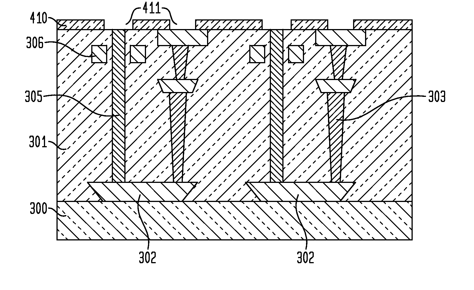
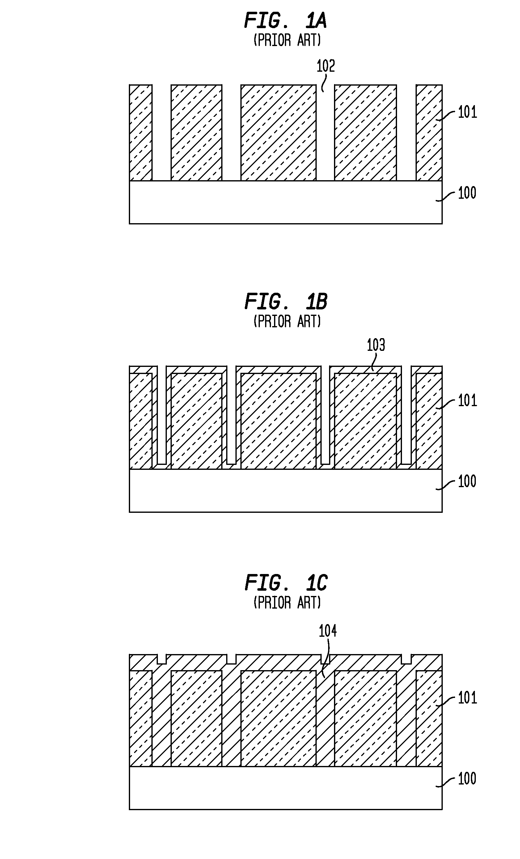
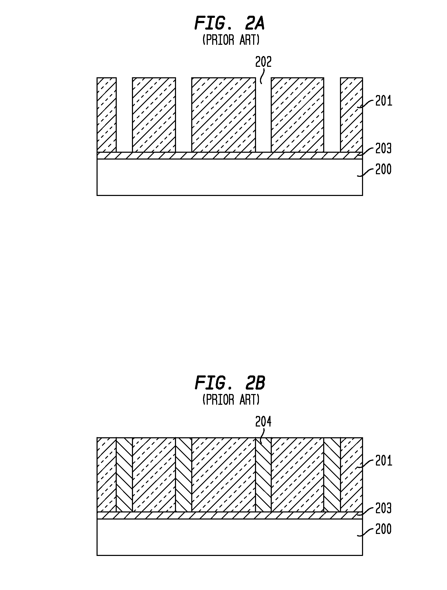
[0028]In the following description, numerous specific details are set forth, such as particular structures, components, materials, dimensions, processing steps and techniques, in order to provide a thorough understanding of the present invention. However, it will be appreciated by one skilled in the art that the invention may be practiced without these specific details or by substituting certain details with known equivalents thereof, without departing from the spirit of the invention. Further, standard structures or processing steps well known to those ordinarily skilled in the art have not been described in detail in order to avoid obscuring the invention.

[0029]It will be understood that when an element as a layer, region or substrate is referred to as being “on” another element, it can be directly on the other element or intervening elements may also be present. In contrast, when an element is referred to as being “directly on” another element, there are no intervening elements p...


PUM

PropertyMeasurementUnit
cross-sectional diameteraaaaaaaaaa
conductivityaaaaaaaaaa

Abstract

The present invention is related to a method for forming vertical conductive structures by electroplating. Specifically, a template structure is first formed, which includes a substrate, a discrete metal contact pad located on the substrate surface, an inter-level dielectric (ILD) layer over both the discrete metal contact pad and the substrate, and a metal via structure extending through the ILD layer onto the discrete metal contact pad. Next, a vertical via is formed in the template structure, which extends through the ILD layer onto the discrete metal contact pad. A vertical conductive structure is then formed in the vertical via by electroplating, which is conducted by applying an electroplating current to the discrete metal contact pad through the metal via structure. Preferably, the template structure comprises multiple discrete metal contact pads, multiple metal via structures, and multiple vertical vias for formation of multiple vertical conductive structures.

Description

CROSS-REFERENCE TO RELATED APPLICATIONS[0001]This application is a divisional of U.S. patent application Ser. No. 11 / 620,497, filed Jan. 5, 2007.[0002]The present application is related to co-pending U.S. patent applications entitled “MEMORY STORAGE DEVICES COMPRISING DIFFERENT FERROMAGNETIC MATERIAL LAYERS, AND METHODS OF MAKING AND USING THE SAME” (Attorney Docket No. YOR20060192US1-SSMP19771) and “FORMATION OF NANOSTRUCTURES COMPRISING COMPOSITIONALLY MODULATED FERROMAGNETIC LAYERS BY PULSED ECD” (Attorney Docket No. YOR20060194US1-SSMP19769), which were filed on even date herewith and are assigned to the same assignee as the present application. The entire contents of such co-pending U.S. patent applications are incorporated herewith by reference for all purposes.BACKGROUND[0003]The present invention relates to formation of vertical devices by electroplating, and more specifically, to formation of vertical structures using electroplating techniques.[0004]Electroplating, which is...

Claims


Application Information

Patent Timeline
Patent Type & Authority Applications(United States)
IPC IPC(8): H01L23/48
CPCH01L21/76879Y10S205/925H01L21/2885G11C11/161H01H51/00H01L21/3205
Inventor DELIGIANNI, HARIKLIAHUANG, QIANGHUMMEL, JOHN P.ROMANKIW, LUBOMYR T.ROTHWELL, MARY B.
Owner GLOBALFOUNDRIES INC
Features
  • R&D
  • Intellectual Property
  • Life Sciences
  • Materials
  • Tech Scout
  • Unparalleled Data Quality
  • Higher Quality Content
  • 60% Fewer Hallucinations
Learn More