Organic light-emitting diode display

a light-emitting diode and organic technology, applied in the direction of discharge tube luminescnet screens, discharge tube/lamp details, organic semiconductor devices, etc., can solve the problem of limited sub-pixel resolution, and achieve the effect of reducing the patterning margin and high resolution

Active Publication Date: 2009-12-03
SAMSUNG DISPLAY CO LTD
View PDF3 Cites 75 Cited by
  • Summary
  • Abstract
  • Description
  • Claims
  • Application Information

AI Technical Summary

Benefits of technology

[0009]Aspects of the present invention provide an OLED display having a high resolution, while maintaining a minimum margin for patterning of an organic emission layer.

Problems solved by technology

A minimum margin is required for patterning sub-pixels, due to limitations of current patterning technology.
Accordingly, the resolution of sub-pixels is limited.

Method used


Image

  • Organic light-emitting diode display
  • Organic light-emitting diode display
  • Organic light-emitting diode display

Examples


Embodiment Construction

[0040]Reference will now be made in detail to the exemplary embodiments of the present invention, examples of which are illustrated in the accompanying drawings, wherein like reference numerals refer to the like elements throughout. The exemplary embodiments are described below, in order to explain the aspects of the present invention, by referring to the figures.

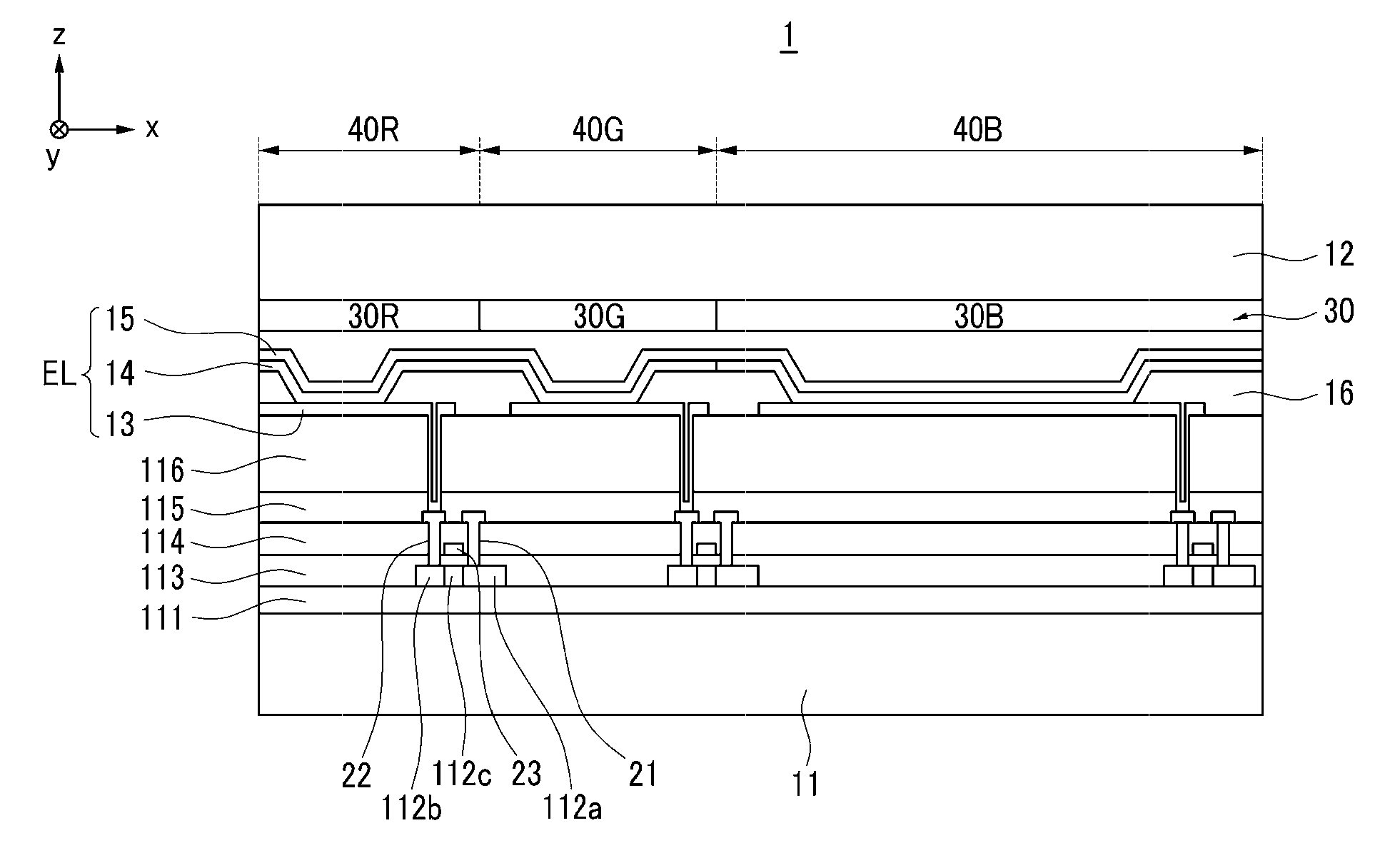
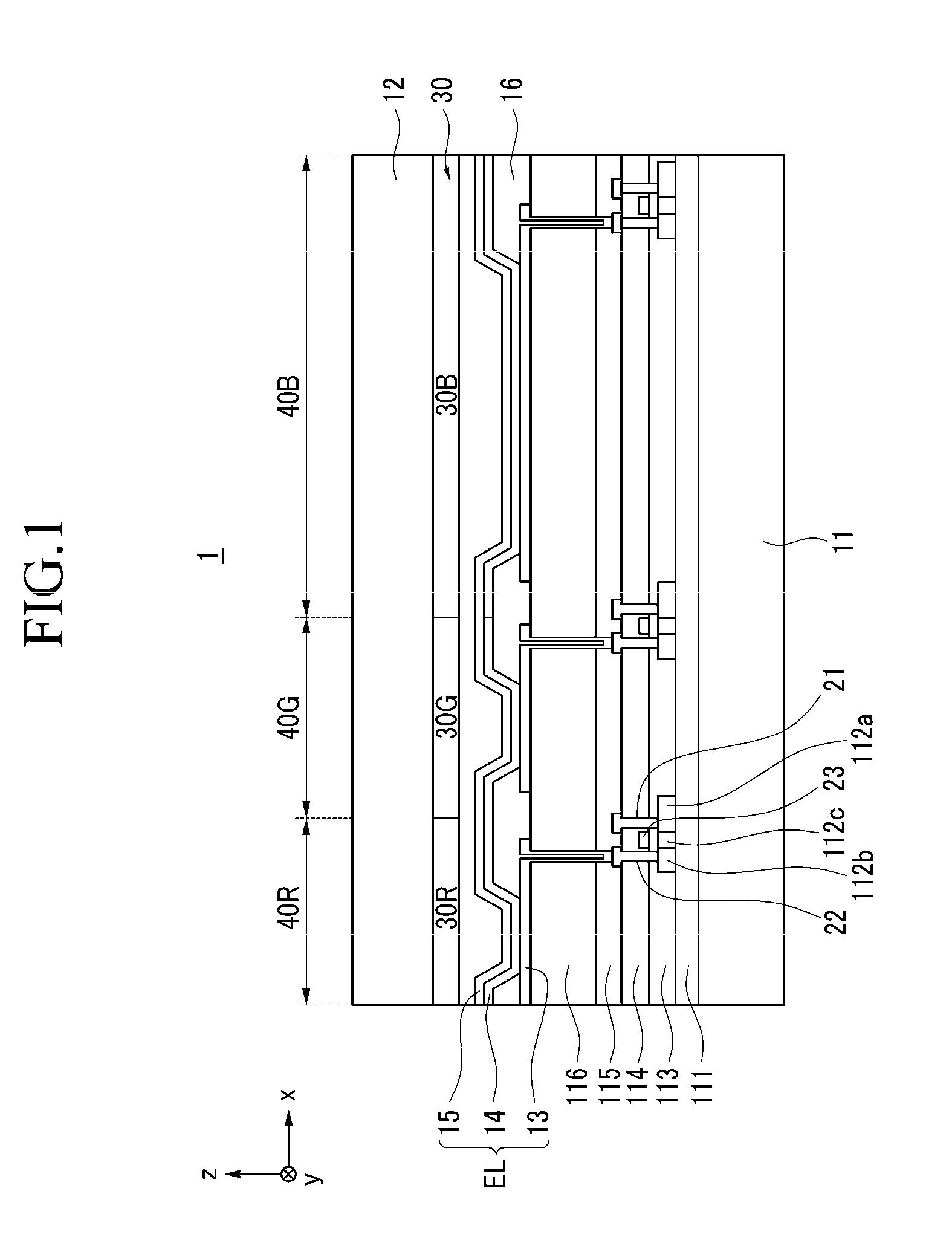
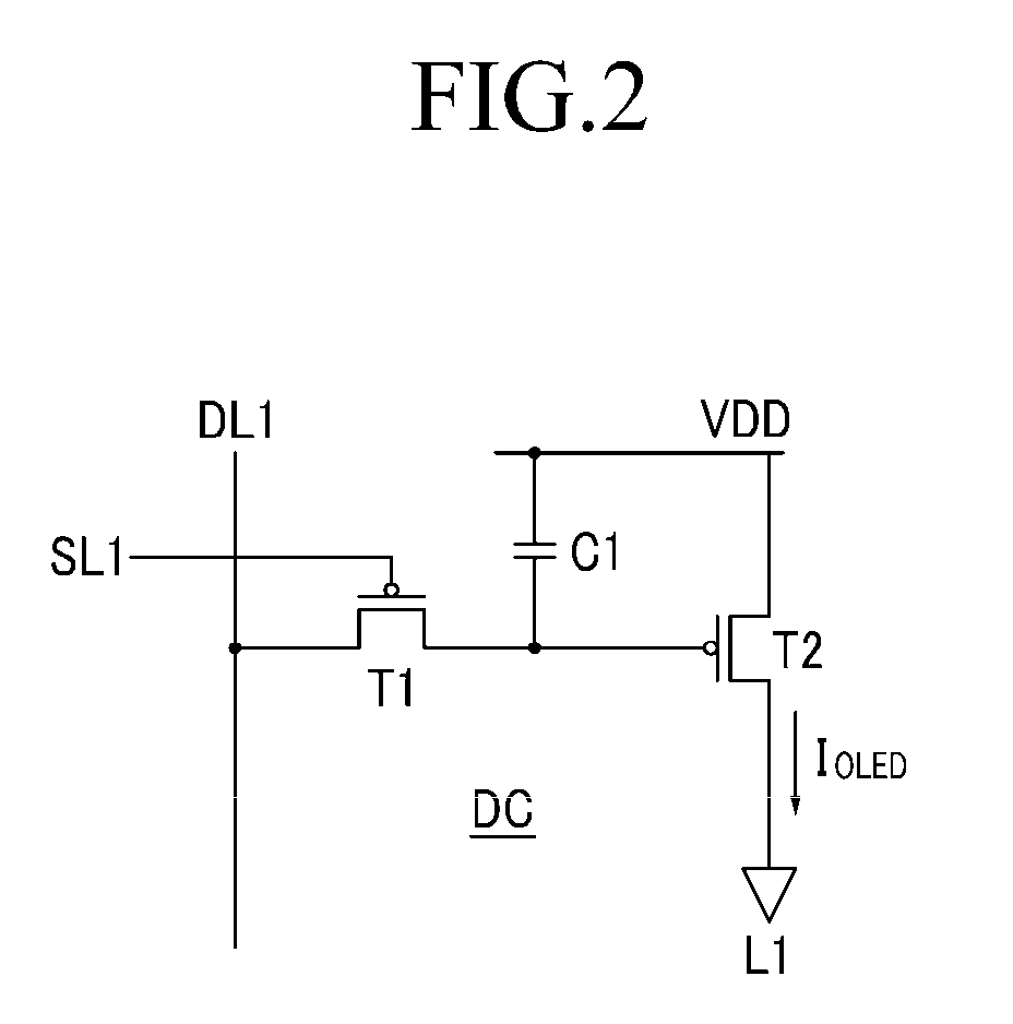
[0041]FIG. 1 is a cross-sectional view of an OLED display 1, according to a first exemplary embodiment of the present invention, and FIG. 2 is a schematic diagram of a sub-pixel circuit structure illustrated in FIG. 1. Referring to FIGS. 1 and 2, the OLED display 1 includes a first substrate 11 (rear substrate), an opposing second substrate 12 (front substrate), and an organic light-emitting unit EL, a driving circuit DC, and a filter 30.

[0042]The organic light-emitting unit EL is formed on a side of the front substrate 12 that faces the rear substrate 11, and includes an anode 13, an organic emission layer 14, and a cathod...


PUM


Abstract

An OLED display including: a first substrate; an opposing second substrate; an organic light-emitting unit disposed on a side of the first substrate that faces the second substrate; a driving circuit disposed on a side of the second substrate that faces the first substrate and connected to the organic light-emitting unit; and a filter. The organic light-emitting unit includes that is an anode, a cathode, and an organic emission layer disposed therebetween. The organic emission layer includes a blue emission layer a yellow emission layer. The filter is to convert light from the yellow emission layer into red light and green light.

Description

CROSS-REFERENCE TO RELATED APPLICATIONS[0001]This application claims the benefit of Korean Patent Application No. 10-2008-0052215, filed in the Korean Intellectual Property Office on Jun. 3, 2008, the disclosure of which is incorporated herein, by reference.BACKGROUND OF THE INVENTION[0002]1. Field of the Invention[0003]Aspects of the present invention relate to an organic light-emitting diode (OLED) display having a high resolution.[0004]2. Description of the Related Art[0005]An OLED display includes organic light-emitting elements, each of which is composed of a hole injection electrode, an organic emission layer, and an electron injection electrode. An OLED display emits light when excitons, which are generated by the combination of electrons and holes, fall from an excited state to a ground state.[0006]An OLED display is self-emissive and does not require an additional light source, as is used in a liquid crystal display (LCD), and thus, has a comparatively reduced thickness and...

Claims


Application Information

Patent Timeline
Patent Type & Authority Applications(United States)
IPC IPC(8): H01J1/63
CPCH01L27/3213H01L2251/5315H01L27/3244H01L27/322Y02E10/549H10K59/351H10K59/352H10K59/38H10K59/12H10K2102/3026H10K59/35H10K77/10
Inventor KIM, EUN-AHKIM, MU-HYUN
Owner SAMSUNG DISPLAY CO LTD
Why Eureka
Try Eureka