

Col (chip-on-lead) multi-chip package
a chip-on-lead and multi-chip technology, applied in the field of chip-on-lead (col) multi-chip packages, can solve the problems of broken wires, inability to balance the upper and lower mold flows, and limited number of chips that can be stacked inside a package, so as to reduce the shifting of leads
- Summary
- Abstract
- Description
- Claims
- Application Information
AI Technical Summary
Benefits of technology
Problems solved by technology
Method used
Image

Examples
Embodiment Construction
[0009]Please refer to the attached drawings, the present invention will be described by means of embodiments below.
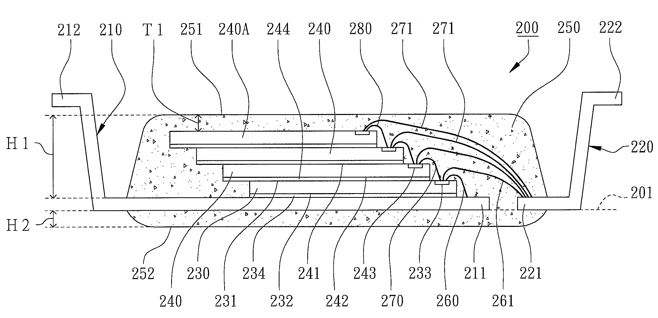
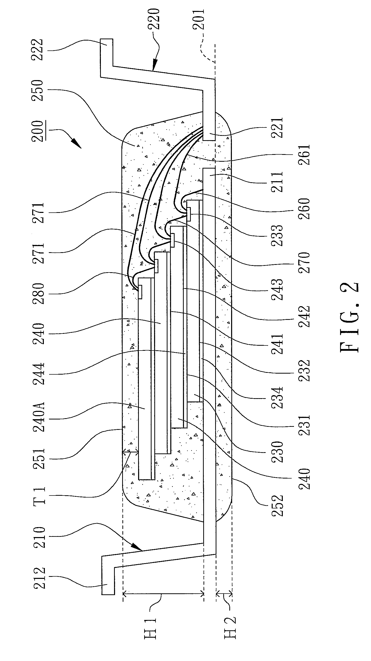
[0010]According to the preferred embodiment of the present invention, a Chip-On-Lead (COL) multi-chip package is revealed in the cross-sectional view of FIG. 2. The COL multi-chip package 200 primarily comprises a plurality of first leads 210, a first chip 230, one or more second chips 240, and an encapsulant 250.
[0011]Each first lead 210 has a first internal lead 211 and a first external lead 212 where the internal leads 211 are portions of the first leads 210 disposed inside the encapsulant 250 and the external leads 212 disposed outside the encapsulant 250. The first leads 210 are parts of a metal leadframe made of iron, copper, or other metal alloy where the first leads 210 have an appropriate thickness such as 0.125 mm or more with enough structural strengths to support the first chip 230 and the second chips 240. Preferably, the thickness of the first lead 210 can...
PUM
 Abstract
Description
Claims
Application Information