High confinement waveguide on an electro-optic substrate

a high confinement waveguide and electro-optic substrate technology, applied in the direction of optical waveguide light guide, optical elements, instruments, etc., can solve the problems of limited electro-optic effect, reduce the mode size of portions, and improve the mode size matching to optical fiber

Inactive Publication Date: 2009-12-31
JDS UNIPHASE CORP
View PDF22 Cites 68 Cited by
  • Summary
  • Abstract
  • Description
  • Claims
  • Application Information

AI Technical Summary

Benefits of technology

[0017]The present invention has found that significant advantage can be obtained by creating high confinement waveguides directly on the electro-optic substrate, such as with SiN:Si on lithium niobate coupled to diffused waveguides such as Ti, or other waveguides within the electro-optic substrate, such as annealed proton exchange (APE) waveguides, in order to reduce the mode size for portions of the waveguide circuit. Generally, the high confinement waveguide will not be the only waveguide in the electro-optic device, because only the tail of the optical mode is transmitted through the electro-optic material in a high confinement waveguide. Consequently, the electro-optic effect is limited. This is acceptable for certain applications. It is preferred to combine the high confinement waveguide for small bend radius areas with Ti diffused waveguides for straight sections and for better mode size matching to optical fiber. Alternatively, a hybrid waveguide in which a high confinement core is coincident with a diffused waveguide of similar refractive indices can be created to provide optical transmission in the electro-optic substrate with a smaller mode size.

Problems solved by technology

Consequently, the electro-optic effect is limited.

Method used


Image

  • High confinement waveguide on an electro-optic substrate
  • High confinement waveguide on an electro-optic substrate
  • High confinement waveguide on an electro-optic substrate

Examples


Embodiment Construction

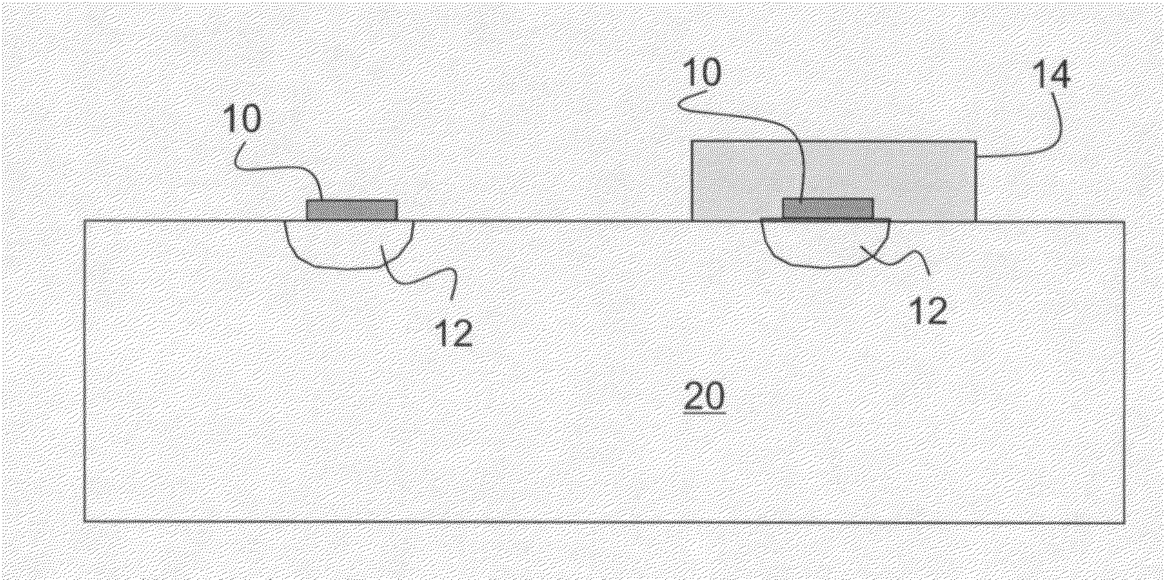
[0055]FIGS. 4-31 describe various embodiments of the invention, which consist of a high confinement waveguide, like SiN:Si, formed on top of an electro-optic material, like lithium niobate (LN). FIGS. 4-6 show the cross sections of different types of SiN:Si-on-LN waveguides. The SiN strip 10 is made to be rich in Si, increasing its optical index of refraction to be slightly higher than the optical index of LN 20. A high confinement waveguide must have an index change relative to the electro-optic substrate that is significantly larger than that created in the diffused waveguide. The maximum refractive index in a diffused waveguide in lithium niobate is typically 0.01 to 0.02 higher than the substrate index or said another way, the index change forming the waveguide is less than 1% of the substrate index. Furthermore, the average index change in most of the waveguide is less than the maximum index change as a result of creating a waveguide with a diffusion process, hence the average ...


PUM


Abstract

The invention relates to an optical device including a passive high confinement waveguide, such as of silicon-rich silicon nitride, on an electro-optic substrate, like lithium niobate, optically coupled to a waveguide in the electro-optic substrate. A wide range of electro-optic devices are enabled by this high confinement waveguide structure, including: directional couplers, compact tap couplers, folded electro-optic devices, electro-optic modulators including ring resonators, electro-optic gratings. Further applications enabled by the present invention include hybrid passive planar lightwave circuits (PLC) integrated with electro-optically active waveguides, using the high confinement waveguide as an intermediary waveguide to transfer optical power between the passive and active components.

Description

TECHNICAL FIELD[0001]The present invention relates to an optical device including a passive high confinement waveguide, such as of silicon-rich silicon nitride, on an electro-optic substrate, like lithium niobate, optically coupled to a waveguide in the electro-optic substrate. A wide range of electro-optic devices are enabled by this high confinement waveguide structure, including: directional couplers, compact tap couplers, folded electro-optic devices, electro-optic modulators including ring resonators, electro-optic gratings. Further applications enabled by the present invention include hybrid passive planar lightwave circuits (PLC) integrated with electro-optically active waveguides, using the high confinement waveguide as an intermediary waveguide to transfer optical power between the passive and active components.BACKGROUND OF THE INVENTION[0002]A high confinement waveguide for use on electro-optic substrates is highly desirable for its ability to increase the bend radius of ...

Claims


Application Information

Patent Timeline
Patent Type & Authority Applications(United States)
IPC IPC(8): G02B6/12
CPCB82Y20/00G02F1/0118G02B6/1228G02B6/1223
Inventor DOUGHERTY, DAVID J.KISSA, KARL
Owner JDS UNIPHASE CORP
Why Eureka
Try Eureka