Organic EL Display Device

a display device and organic technology, applied in the direction of discharge tube luminescnet screens, discharge tube/lamp details, electric discharge lamps, etc., can solve the problems of reducing the resistance in the upper electrode, affecting and affecting the effect of the brightness of the screen

Active Publication Date: 2010-01-14
SAMSUNG DISPLAY CO LTD +1
View PDF4 Cites 13 Cited by
  • Summary
  • Abstract
  • Description
  • Claims
  • Application Information

AI Technical Summary

Benefits of technology

[0024]According to the invention, it is possible to realize an organic EL display device that can suppress the shading phenomenon while keeping a screen brightness by changing a film thickness of the upper electrode for every pixel. Further, according to the invention, it is possible to realize an organic EL display device with a high brightness that can suppress the light absorption of the upper electrode on the whole, by suppressing the film thickness of the upper electrode only for the blue pixel small and enlarging the film thicknesses of the upper electrodes for the red pixel and the green pixel.

Problems solved by technology

The light passing through the respective color filters is different in wavelength and depending on a thickness of the opposite electrode, specified wavelengths interfere with each other, hence to deteriorate the emitting efficiency in some cases.
On the other hand, in the organic EL display device of a current driven type, a voltage drop in the upper electrode becomes a problem.
A metal film of low resistance can be used for the upper electrode; however, a metal film has to be extremely thin in order to keep transparency, which does not contribute to reducing a resistance in the upper electrode.

Method used


Image

  • Organic EL Display Device
  • Organic EL Display Device
  • Organic EL Display Device

Examples


embodiment 1

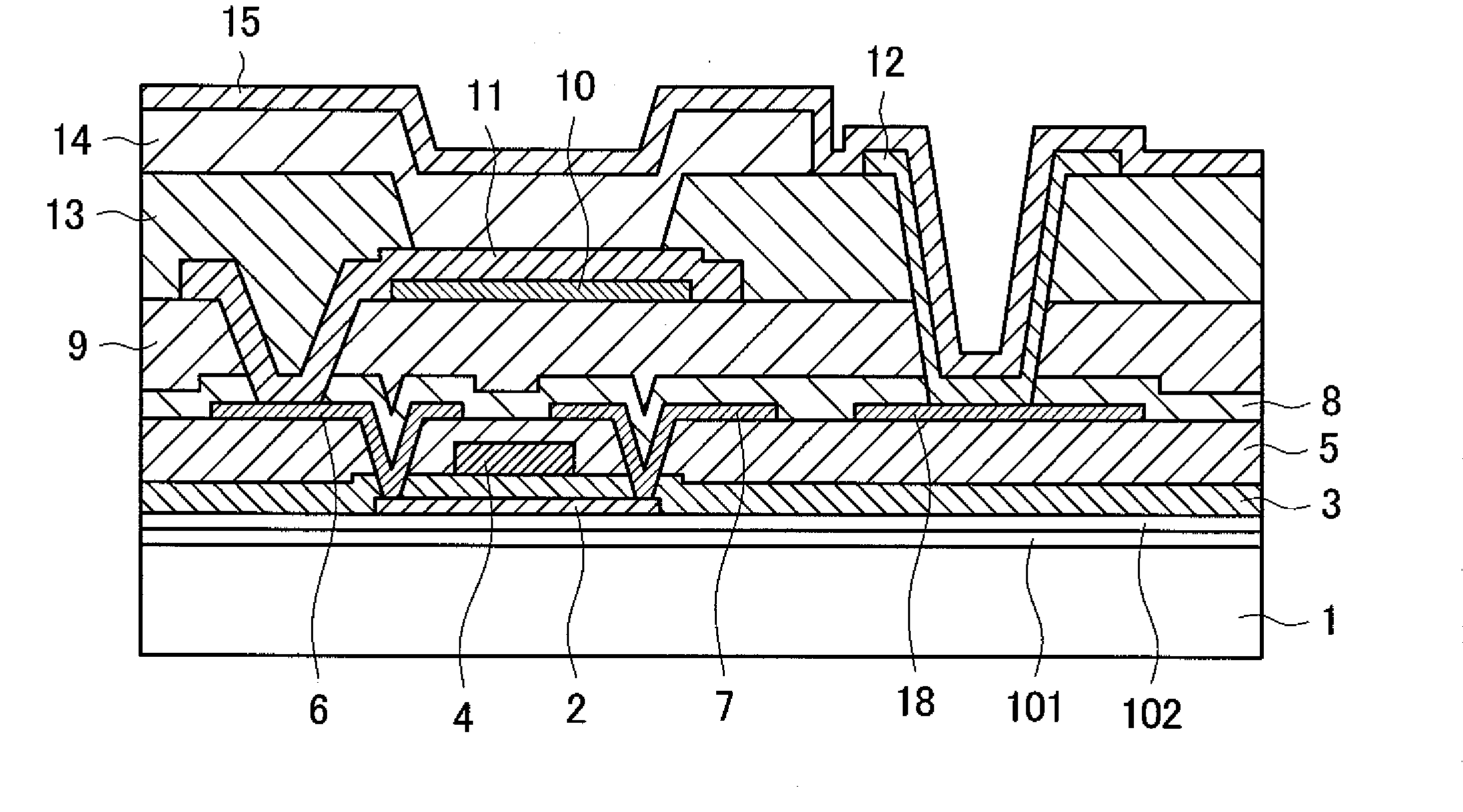
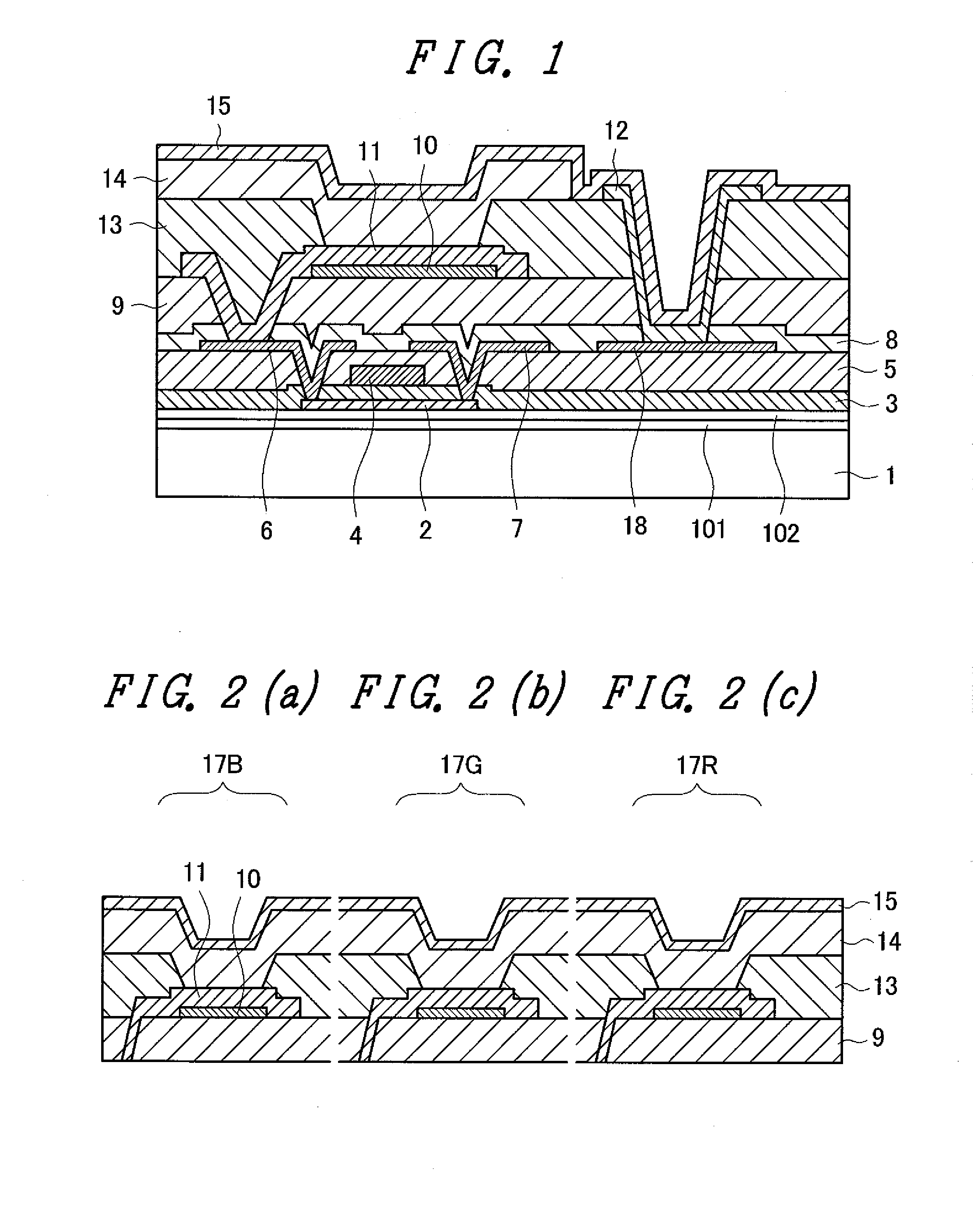
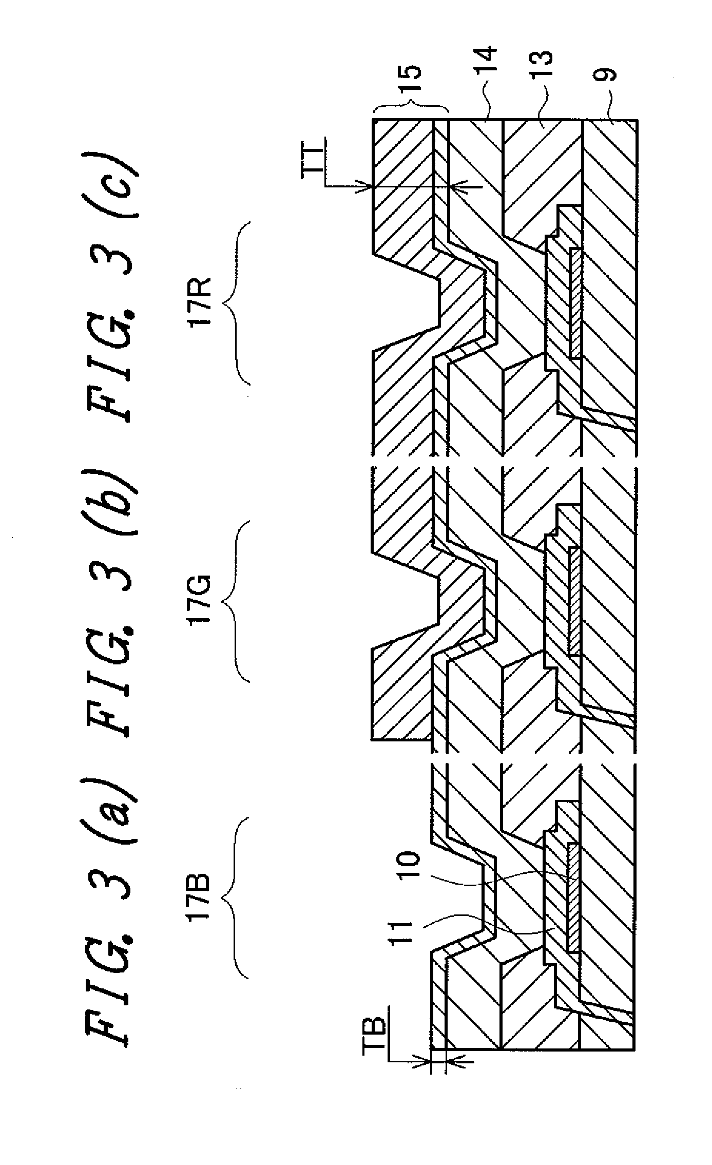
[0062]FIG. 3A, FIG. 3B, and FIG. 3C are cross sectional schematic views showing the first embodiment of the invention. FIG. 3A is a cross sectional view of a blue pixel 17B, FIG. 3B is a cross sectional view of a green pixel 17G, and FIG. 3C is a cross sectional view of a red pixel 17R. This embodiment is characterized in that the respective upper electrodes 15 for the red pixel 17R and the green pixel 17G are thicker than the upper electrode 15 for the blue pixel 17B.

[0063]Light absorption of InZnO used as the upper electrode 15 is greater according as the wavelength of light is shorter. FIG. 4 shows a light transmittance of InZnO in every wavelength; the horizontal axis indicates a light wavelength λ (nm), while the vertical axis indicates a light transmittance I / Io. The transmittance in the case where a film thickness is a specified value B, is shown by a black circle and the transmittance in the case where a film thickness becomes ten times as large as the specified value B, is ...

embodiment 2

[0075]The first embodiment reduces the shading by enlarging the respective film thicknesses of the respective upper electrodes 15 for the red pixel 17R and the green pixel 17G without enlarging the film thickness of the upper electrodes 15 for the blue pixel 17B. In the first embodiment, the film thickness for the red pixel 17R is equal to the film thickness for the green pixel 17G. The first embodiment has an advantage that only one additional sputtering can reduce the shading without actual deterioration in brightness because the film thickness for the red pixel 17R is equal to that for the green pixel 17G.

[0076]On the other hand, as illustrated in FIG. 4, the transmittance of the upper electrode 15 is greater in the short wavelength region. Therefore, from the view point of properties, it is the most rational to make the upper electrode 15 for the red pixel 17R thicker than the upper electrode 15 for the green pixel 17G. Also in this case, since the upper electrode 15 is not thic...

embodiment 3

[0080]This embodiment relates to the case where the film thickness of the upper electrode 15 is enlarged either in the red pixel 17R or the green pixel 17G. When the film thickness of the upper electrode 15 changes, the light interference effect varies. The most suitable film thickness for taking out light depends on light wavelength. Therefore, when the film thicknesses of the upper electrodes 15 are enlarged in all the pixels including the red pixel 17R, the green pixel 17G, and the blue pixel 17B, the interference effect varies depending on the color.

[0081]As having been described in the first embodiment, when the film thickness of the upper electrode 15 for the blue pixel 17B is also enlarged, the brightness deteriorates. Further, like the second embodiment, when the film thicknesses for the red pixel 17R and the green pixel 17G are varied from each other, additional sputtering has to be performed two times. In this embodiment, additional sputtering is reduced to one time and th...


PUM


Abstract

In a top emission type organic EL display device, brightness gradient in a screen is reduced while keeping a screen brightness. A reflection film is formed under a lower electrode and the light from an organic EL layer is emitted through an upper electrode. Light absorption of the upper electrode is larger on the side of a shorter wavelength. When a film thickness of the upper electrode is enlarged in order to reduce the brightness gradient in a screen, the film thicknesses of the upper electrodes for a red pixel and a green pixel are enlarged without enlarging the film thickness of the upper electrode for a blue pixel. This makes it possible to reduce the brightness gradient as well as to suppress the light absorption of the upper electrode.

Description

CROSS-REFERENCE TO RELATED APPLICATIONS[0001]The present application claims priority from Japanese Application JP 2008-179066 filed on Jul. 9, 2008, the content of which is hereby incorporated by reference into this application.BACKGROUND OF THE INVENTION[0002]1. Field of the Invention[0003]The present invention relates to an organic EL display device, and more particularly, to a top emission type organic EL display device which has a high and uniform brightness in its screen.[0004]2. Background Art[0005]Organic EL display device is classified into a bottom emission type which takes out light emitted from an organic EL layer in the direction of glass substrate on which the organic EL layer and the like are formed and a top emission type which takes out the light in the direction opposite to the glass substrate on which the organic EL layer and the like are formed. The top emission type has an advantage that the respective organic EL layers can ensure a large area, thus increasing th...

Claims


Application Information

Patent Timeline
Patent Type & Authority Applications(United States)
IPC IPC(8): H01L51/52
CPCH01L27/3211H01L27/3244H01L51/5203H01L51/0079H01L51/0072H10K59/35H10K59/12H10K85/321H10K85/6572H10K50/824H10K59/805H10K50/805
Inventor TOYODA, HIRONORITANAKA, MASAHIROOKUNAKA, MASAAKIGUNJI, MASAKAZU
Owner SAMSUNG DISPLAY CO LTD
Why Eureka
Try Eureka