Resistive nonvolatile memory element, and production method of the same

a non-volatile, memory element technology, applied in the direction of digital storage, instruments, semiconductor devices, etc., can solve the problems of increasing the variation among each element, insufficient accuracy of these process techniques, and inability to manufacture micro-fabricated elements, etc., to achieve a simple and convenient process

Inactive Publication Date: 2010-01-14
PANASONIC CORP
View PDF3 Cites 16 Cited by
  • Summary
  • Abstract
  • Description
  • Claims
  • Application Information

AI Technical Summary

Benefits of technology

[0046]According to the resistive nonvolatile memory element of the present invention, a resistive nonvolatile memory element is enabled having an electric cu...

Problems solved by technology

When the accuracy of these process techniques is insufficient, production of the micro-fabricated element would be difficult.
In addition, low reproducibility in producing the nanost...

Method used


Image

  • Resistive nonvolatile memory element, and production method of the same
  • Resistive nonvolatile memory element, and production method of the same
  • Resistive nonvolatile memory element, and production method of the same

Examples


embodiments

[0063]The method for production of a resistive nonvolatile memory element of the present invention is first explained.

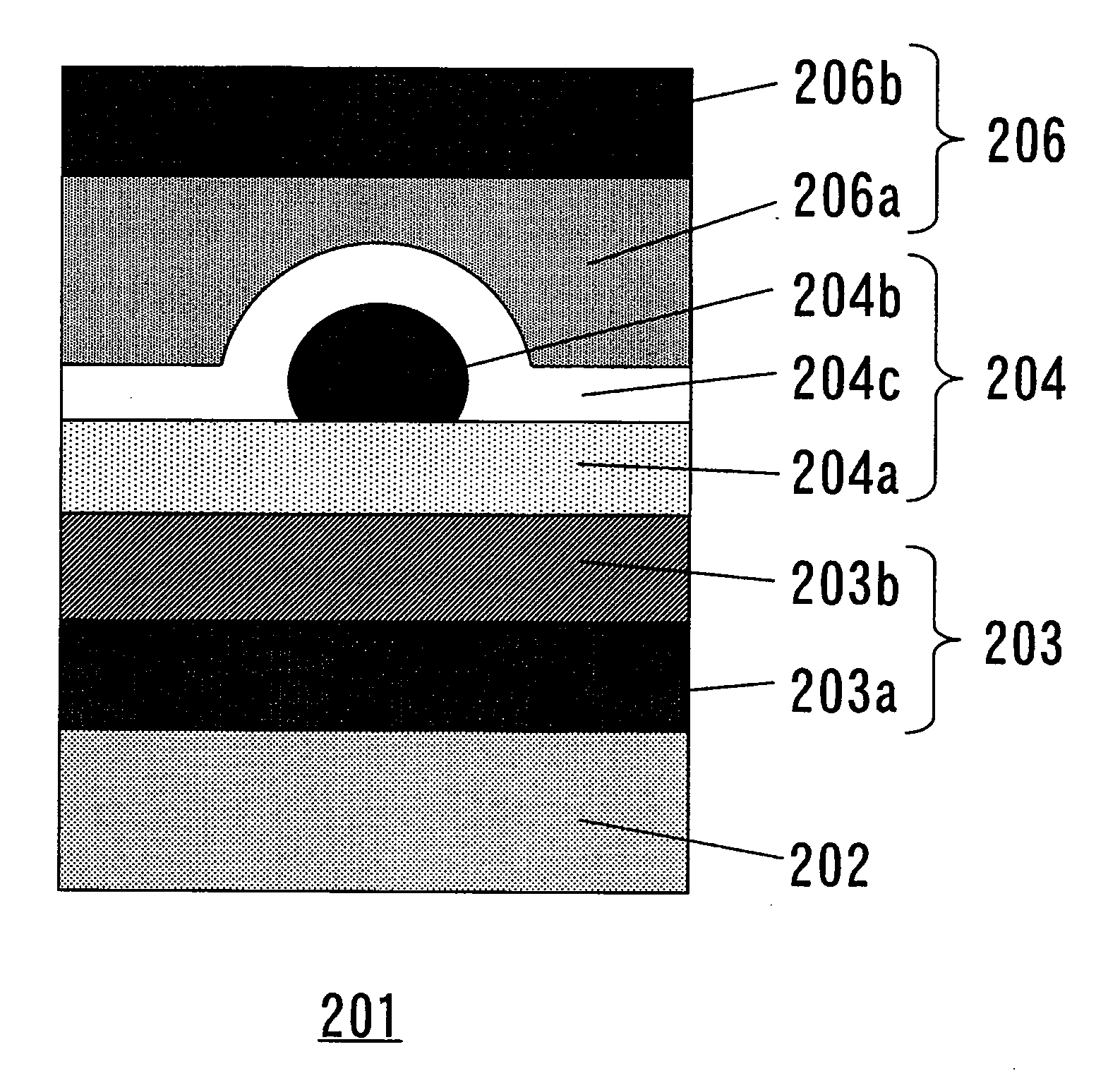
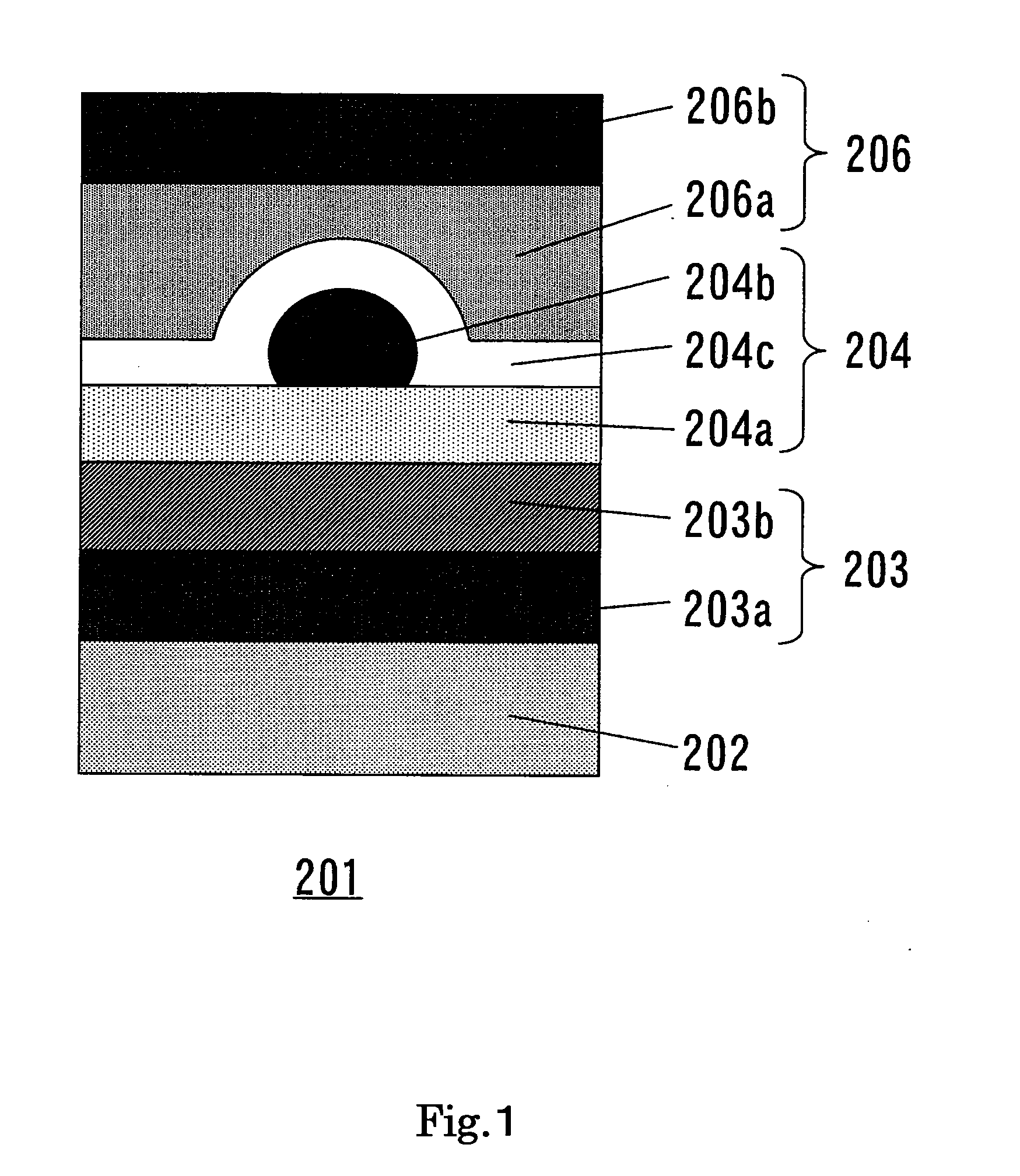
[0064]In this Embodiment, as shown in FIG. 6 and FIG. 7, after first electrode 203 is formed on the surface of substrate 202 in the “first electrode formation step” (FIG. 7(a)), oxide semiconductor layer 204a the resistance of which is altered depending on the applied voltage is formed on the first electrode 203 in an “oxide semiconductor layer formation step” (FIG. 7(b)); ferritin 205 constituted with metal compound core 205a and protein 205b on the external side thereof is arranged on the oxide semiconductor layer 204a in a “ferritin arranging step” (FIG. 7(c)); protein 205b on the external side of the ferritin 205 is removed to modify the metal compound core 205a into metal nanoparticle 204b in a “protein removal and core modification step” (FIG. 7(d)); tunnel barrier layer 204c is formed on the oxide semiconductor layer 204a and on the metal nanoparticles 204b in...

example 1

[0089]Hereinafter, a method for production of the resistive nonvolatile memory element of the Example 1 is explained in detail.

[0090]Introduction of Gold Sulfide Core into Apoferritin

[0091]Operation for introducing a gold sulfide core into a cavity inside apoferritin is first explained below.

[0092]First, 17 mg of thiourea was added to 1 mL of a 20 mM potassium chloroaurate (KAuCl4) solution, followed by mixing.

[0093]Several minutes later, thus yielded yellowish solution of an Au (III) ion was turned to a colorless transparent solution of a Au (I)-thiourea complex, and the solution was adjusted to a 20 mM gold thiourea complex solution.

[0094]Next, in a phosphate buffer (pH 8), a solution of purified apoferritin derived from horse, and the aforementioned gold thiourea complex solution were mixed.

[0095]In this step, the resultant final mixed solution was adjusted to have a phosphate buffer concentration of 50 mM, a thiourea concentration of 3 mM, and a concentration of apoferritin deri...


PUM


Abstract

An object of the present invention is to provide a resistive nonvolatile memory element having an electric current path which can be realized by a simple and convenient process, and capable of allowing for micro-fabrication.
The resistive nonvolatile memory element of the present invention includes first electrode 203, oxide semiconductor layer 204a which is formed on the first electrode 203 and the resistance of which is altered depending on the applied voltage, metal nanoparticles 204b having a diameter of between 2 nm and 10 nm arranged on the oxide semiconductor layer 204a, tunnel barrier layer 204c formed on the oxide semiconductor layer 204a and on the metal nanoparticles 204b, and second electrode 206 formed on the tunnel barrier layer 204c, in which the metal nanoparticles 204b are in contact with the oxide semiconductor layer 204a.

Description

BACKGROUND OF THE INVENTION[0001]1. Field of the Invention[0002]The present invention relates to a resistive nonvolatile memory element in which nanoparticles are used, and a method for producing the element in which a protein-inorganic nanoparticle complex is used.[0003]2. Related Art[0004]Although resistive memory elements are expected as one of novel nonvolatile memory elements, problems of needs for forming process (process of applying a high voltage after producing the element to initialize the characteristics of the element), and a large variation of characteristics among the elements are often caused. The forming process is considered as a process for forming a local electric current path inside the element, and the differences of the states of the produced electric current paths are believed to be responsible for such variation of characteristics. In addition, reduction of the electric current value required for the memory operation would be preferable since electric power c...

Claims


Application Information

Patent Timeline
IPC IPC(8): G11C11/00H01L47/00H01L21/16G11C7/00
CPCG11C13/0002G11C2213/15G11C2213/34H01L27/101H01L45/12H01L45/146H01L45/1633Y10S977/773Y10S977/81Y10S977/943H01L45/04H01L45/1246H10N70/801H10N70/20H10N70/828H10N70/028H10N70/8833
Inventor YOSHII, SHIGEOYAMASHITA, ICHIRO
Owner PANASONIC CORP
Why Eureka
Try Eureka