

Lid edge capping load
a capping load and edge technology, applied in the direction of electrical apparatus construction details, chemistry apparatus and processes, bandages, etc., can solve the problems of moisture or temperature-induced thermal degradation, prevent reliable low-temperature operation of electronic packages, and structure can suffer from a moisture-induced shape flattening mechanism
- Summary
- Abstract
- Description
- Claims
- Application Information
AI Technical Summary
Problems solved by technology
Method used
Image

Examples
Embodiment Construction
herein
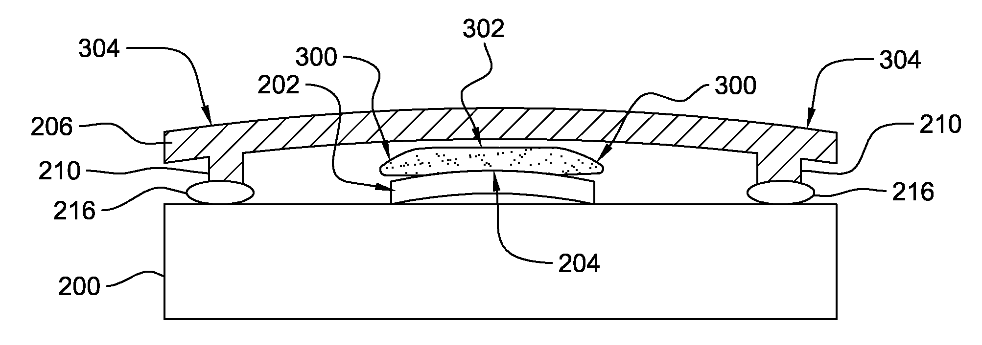
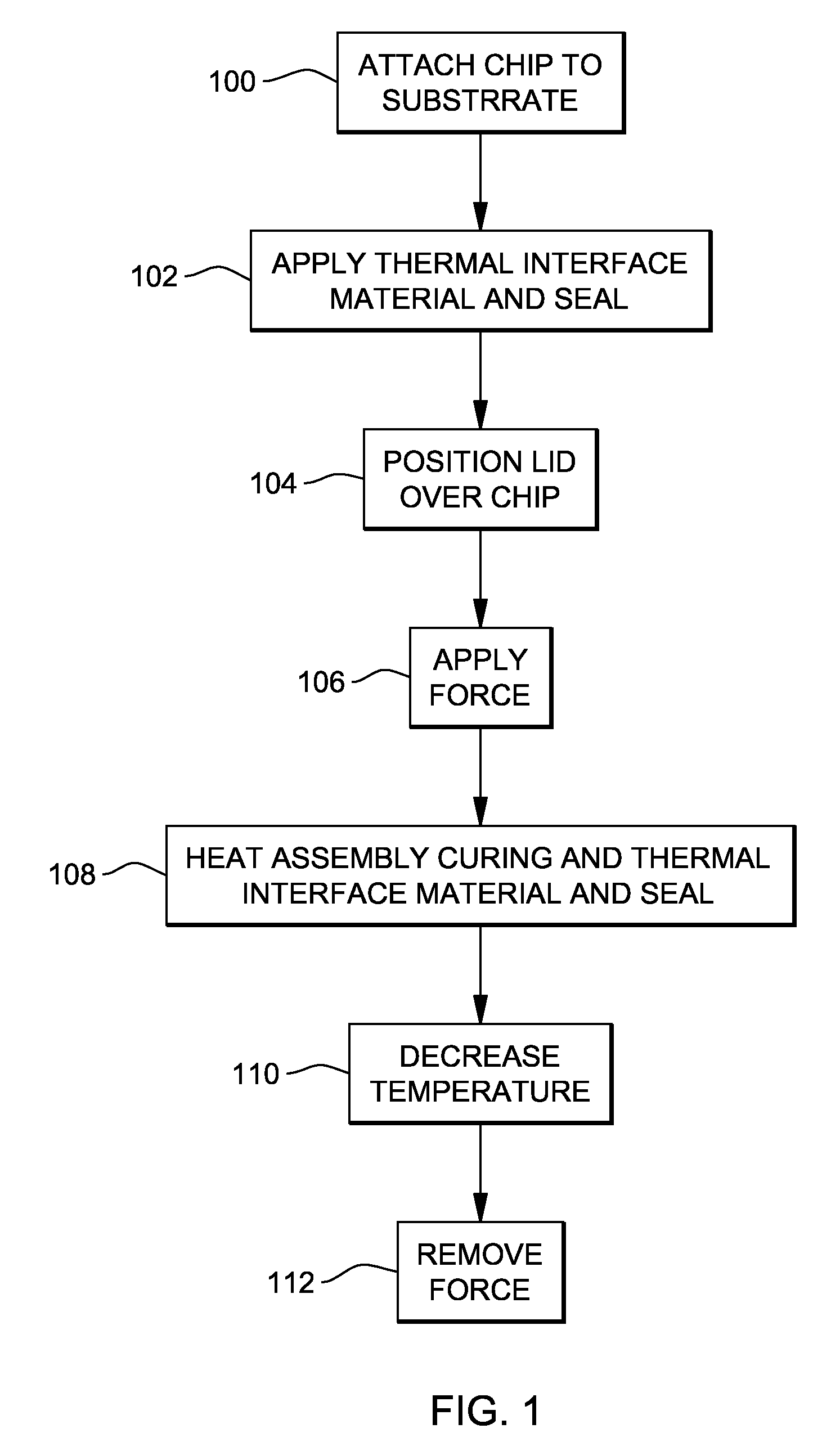
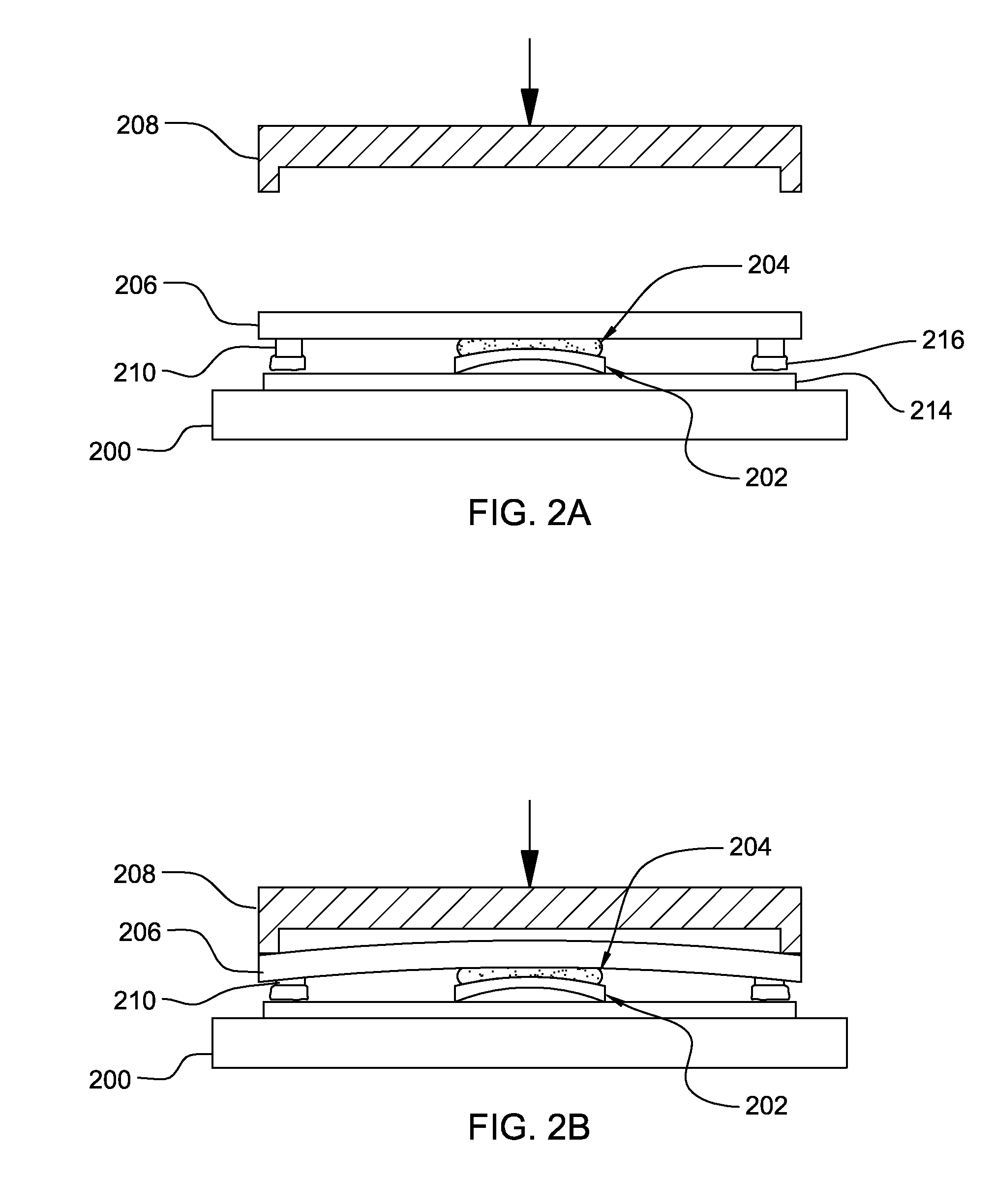
[0002]The embodiments of the embodiments herein generally relate to preventing damage to the thermal interface materials that exist between semiconductor chips and lids which are positioned above the chips, and, more particularly, to a structure and method that causes the thermal interface material to have different regions of compression.
[0003]2. Description of the Related Art
[0004]Integrated circuit structures are commonly formed on wafers which are divided into chips. These chips are usually mounted on substrates and are connected to cooling mechanisms using items such as thermal pastes. One issue that arises with such structures relates to moisture or temperature-induced thermal degradation in the thermal interface material (TIM) that is usually positioned between the chip and the overlying cap or lid. This moisture or temperature thermal degradation prevents reliable low-temperature operation of the electronic package throughout its field life.
[0005]For example, such stru...
PUM
| Property | Measurement | Unit |
|---|---|---|
| thickness | aaaaa | aaaaa |
| temperature | aaaaa | aaaaa |
| temperature | aaaaa | aaaaa |
Abstract
Description
Claims
Application Information