

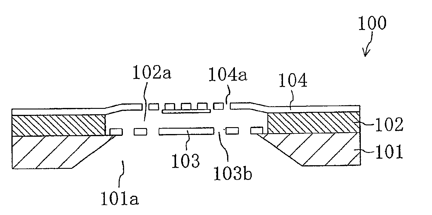
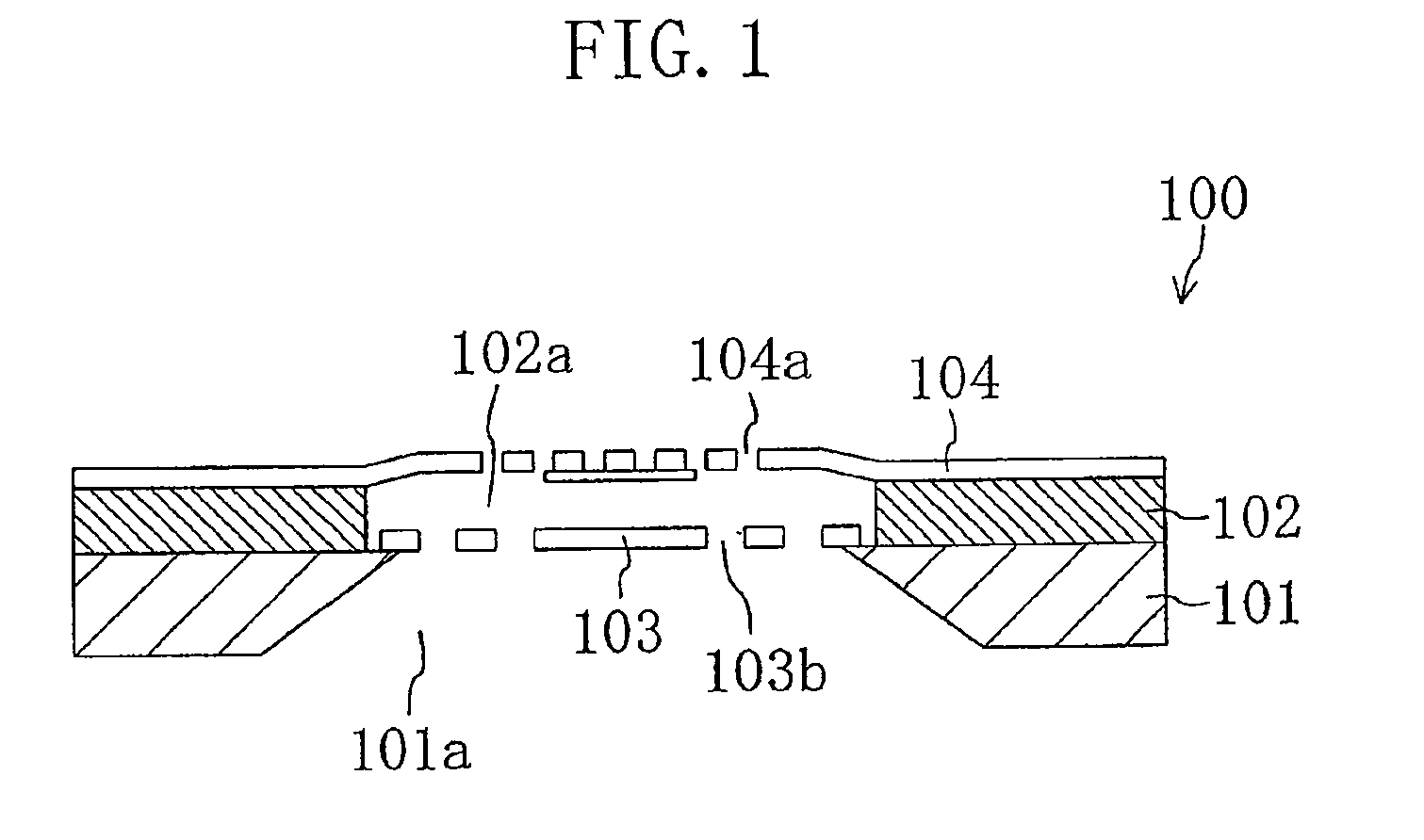
Method for fabricating semiconductor device
a technology of semiconductor devices and fabrication methods, applied in metal working devices, manufacturing tools, welding/soldering/cutting articles, etc., can solve the problems of affecting the function of semiconductor devices, affecting so as to avoid the influence of the etching of the side surface of the groove, the effect of reliably fabricated
- Summary
- Abstract
- Description
- Claims
- Application Information
AI Technical Summary
Benefits of technology
Problems solved by technology
Method used
Image

Examples
first embodiment
Modification of First Embodiment
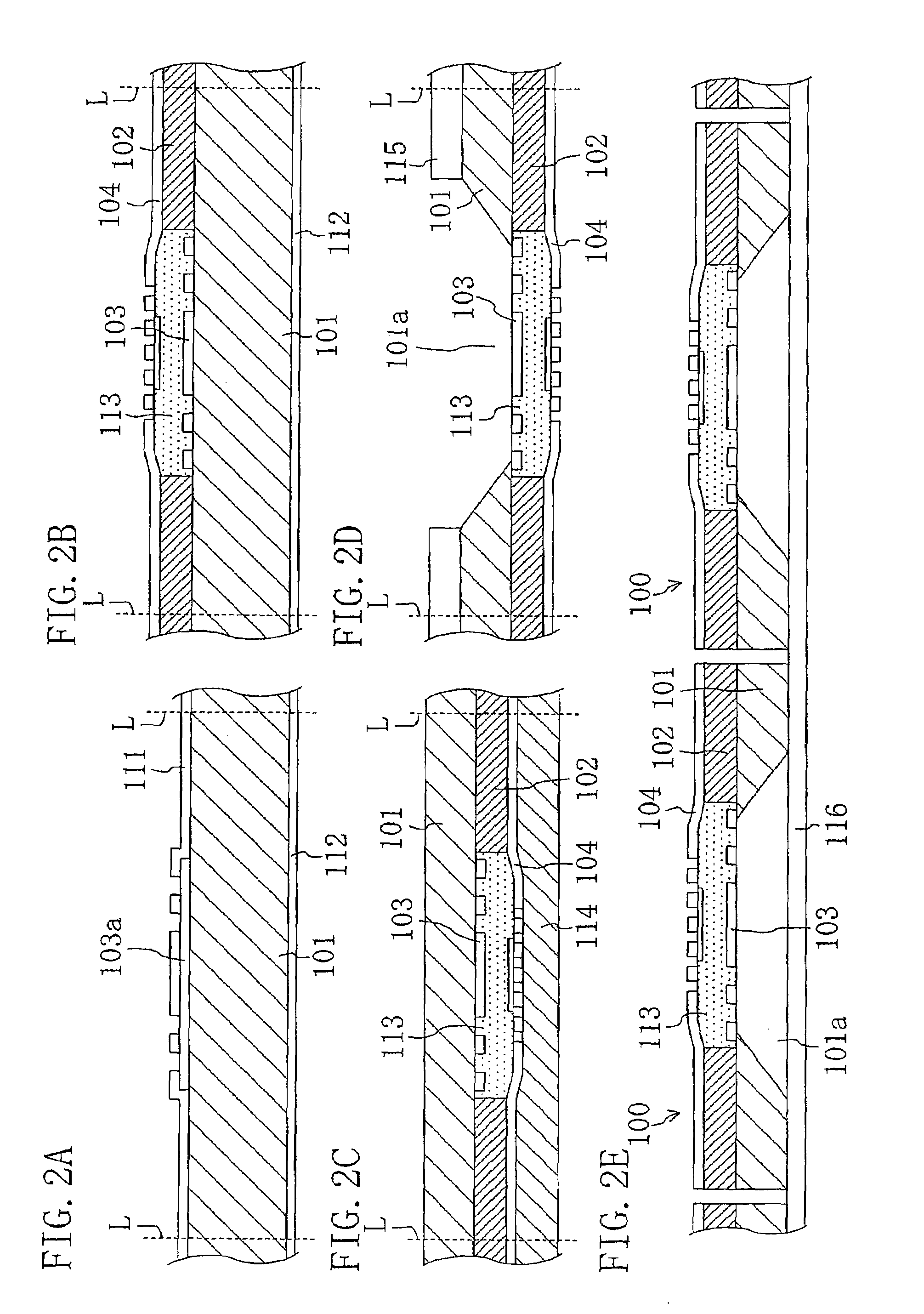
[0084]Next description will be made of a method for fabricating a semiconductor device according to a modification of the first embodiment. When compared with the method for fabricating a semiconductor device according to the first embodiment, this modification is characterized in that a protective film is provided on the fixed film 104. This will now be described with reference to the accompanying drawings. FIGS. 3A and 3B are views showing characteristic processes in this modification.
[0085]First, as in the case of the first embodiment, the steps illustrated in FIGS. 2A to 2D are carried out. Then, as shown in FIG. 3A, a protective film 117 is formed on the fixed film 104, and the dicing tape 116 is stuck onto the back surface of the semiconductor wafer 101. Thereafter, the semiconductor wafer 101 as well as the protective film 117 is subjected to blade dicing along the cutting line L to provide the chips 100a as shown in FIG. 3B. With this method, ...
second embodiment
Modification of Second Embodiment
[0106]A modification of the second embodiment will be described below. FIGS. 6A to 6C are views illustrating semiconductor device fabrication steps according to this modification. In this modification, like the first embodiment, the procedure up to formation of the fixed film 104 is first carried out to provide the structure shown in FIG. 2B.
[0107]Next, a mask 115 is formed on the back surface of the semiconductor wafer 101, and the semiconductor wafer 101 is etched from the back-surface side. Thereby, a through hole 101b is formed, so that the vibrating film 103 is exposed with the back surface facing the through hole 101b. This state is shown in FIG. 6A.
[0108]Subsequently, as shown in FIG. 6B, the sacrifice layer 113 is removed by etching. Thus, the remaining space serves as the cavity 102a. Thereafter, as shown in FIG. 6C, the surface protective tape 119 is stuck onto the fixed film 104, and then the back surface of the semiconductor wafer 101 is ...
third embodiment
[0111]A method for fabricating a semiconductor device according to a third embodiment of the present invention will be described below with reference to the accompanying drawings. Also in the third embodiment, description will be made by using as an example the MEMS microphone chip 100 shown in FIG. 1. Since process steps except removal of the sacrifice layer 113 and chip formation are the same as those of the first embodiment, the chip formation process will be described mainly in the third embodiment. Note that FIGS. 7A to 7C, 8A, and 8B are views illustrating a method for fabricating a semiconductor device according to the third embodiment.
[0112]To be more specific, first, process steps shown in FIGS. 2A to 2D are carried out in the same manner as the first embodiment. Thereby, the semiconductor wafer 101 as shown in FIG. 2D can be provided which has a plurality of structures having the fixed film 104 formed over the vibrating film 103 with the sacrifice layer 113 interposed ther...
PUM
| Property | Measurement | Unit |
|---|---|---|
| width | aaaaa | aaaaa |
| crystalline structure | aaaaa | aaaaa |
| insulating | aaaaa | aaaaa |
Abstract
Description
Claims
Application Information