

Substrate Isolation For Low-Loss Radio Frequency (RF) Circuits
a radio frequency (rf) circuit and substrate isolation technology, applied in the direction of semiconductor devices, semiconductor/solid-state device details, electrical apparatus, etc., can solve problems such as difficulty in achieving, and achieve the effect of reliable fabrication
- Summary
- Abstract
- Description
- Claims
- Application Information
AI Technical Summary
Benefits of technology
Problems solved by technology
Method used
Image

Examples
Embodiment Construction
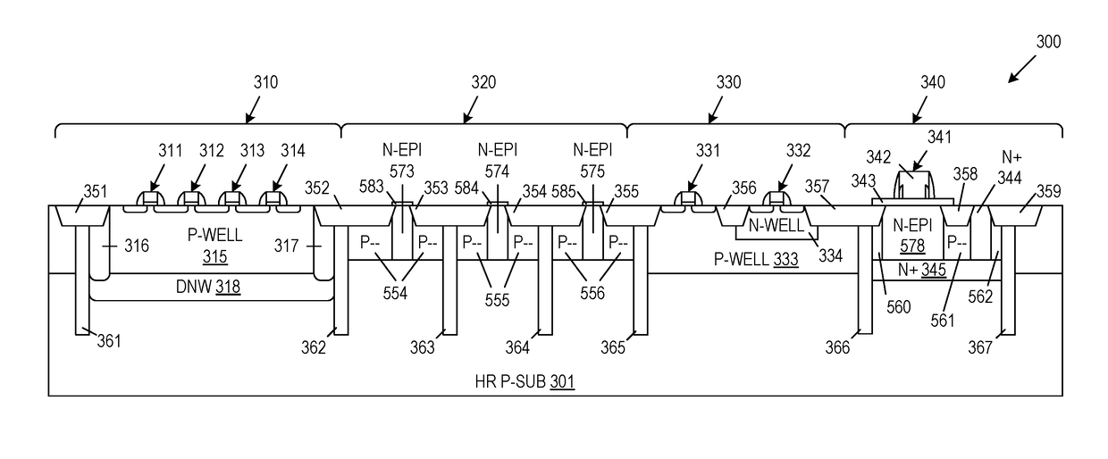
[0040]In general, the present invention uses a grid of deep trench isolation (DTI) regions to isolate active devices fabricated in a semiconductor substrate. The grid of DTI regions also isolates the semiconductor substrate from passive devices fabricated over the semiconductor substrate. In one embodiment, the grid of DTI regions isolates active and passive devices fabricated in accordance with a CMOS process. In another embodiment, the grid of DTI regions isolates active and passive devices fabricated in accordance with a SiGe BiCMOS process. In this embodiment, isolation provided by the grid of DTI regions largely mitigates the parasitic low-impedance path normally provided by the epitaxial layer of the SiGe BiCMOS process, effectively restoring the benefits of the high-resistivity substrate. The present invention will now be described in more detail.
[0041]FIG. 3A is a cross sectional representation of a semiconductor structure 300 in accordance with one embodiment of the present...
PUM
 Abstract
Description
Claims
Application Information