Buried solder bumps for AC-coupled microelectronic interconnects

a microelectronic and interconnect technology, applied in the field of microelectronic devices, can solve the problems of increasing the difficulty of providing a sufficient quantity of high-performance interconnects, the difficulty of providing this close spacing/alignment between closely spaced apart ac-coupled interconnect elements, and the density of interconnects/performance may be a limiting factor, etc., to achieve the effect of high volume, high inductance, and reliable fabrication

Inactive Publication Date: 2005-03-03
NORTH CAROLINA STATE UNIV
View PDF5 Cites 5 Cited by
  • Summary
  • Abstract
  • Description
  • Claims
  • Application Information

AI Technical Summary

Benefits of technology

[0005] Embodiments of the present invention can use buried solder bumps to provide spacing for AC-coupled microelectronic interconnects. Buried solder bumps, according to embodiments of the invention, can provide means for maintaining first and second AC-coupled interconnect elements spaced apart from one another by a distance that is less than the solder bump thickness. Thus, relatively thick solder bumps can be used to maintain sufficient compliance while maintaining the AC-coupled microelectronic interconnects in closely spaced apart relation and / or alignment.
[0013] According to yet other embodiments of the invention, inductive coupling may be used for microelectronic signal interconnects, without the need for buried solder bumps. In these embodiments, a first microelectronic substrate includes a first face and a first inductor on the first face. A digital signal driver is included in the first microelectronic substrate that is configured to drive the first inductor with a digital signal. A second microelectronic substrate includes a second face and a second inductor on the second face that is closely spaced apart from the first inductor. A digital signal receiver in the second microelectronic substrate is configured to receive the digital signal from the digital signal driver via inductive coupling between the first and second inductors. The first and second inductors also may include capacitance associated therewith. When the first microelectronic substrate is an integrated circuit, and the second microelectronic substrate is a second level package for the integrated circuit, the second inductor can have greater inductance than the first inductor. The digital signal receiver can be a DC-offset compensating digital signal receiver, and / or the digital signal driver can be a current mode digital signal driver, as was described above. Accordingly, high performance AC-coupled microelectronic interconnects may be provided that can be fabricated reliably in a high volumes.

Problems solved by technology

As the integration density of microelectronic devices continues to increase, it may become increasingly difficult to provide a sufficient quantity of high performance interconnects that connect the microelectronic device to a next level package.
Accordingly, the interconnect density and / or performance may be a limiting factor in the further integration of microelectronic devices.
However, it may be difficult to provide this close spacing / alignment between the closely spaced apart AC-coupled interconnect elements in a reliable and / or repeatable manner.
It also may be difficult to couple DC power, such as a power supply voltage and / or ground voltage, across the AC-coupled interconnect elements.
Finally, the capacitive coupling may present an excessively high equivalent impedance.

Method used


Image

  • Buried solder bumps for AC-coupled microelectronic interconnects
  • Buried solder bumps for AC-coupled microelectronic interconnects
  • Buried solder bumps for AC-coupled microelectronic interconnects

Examples


Embodiment Construction

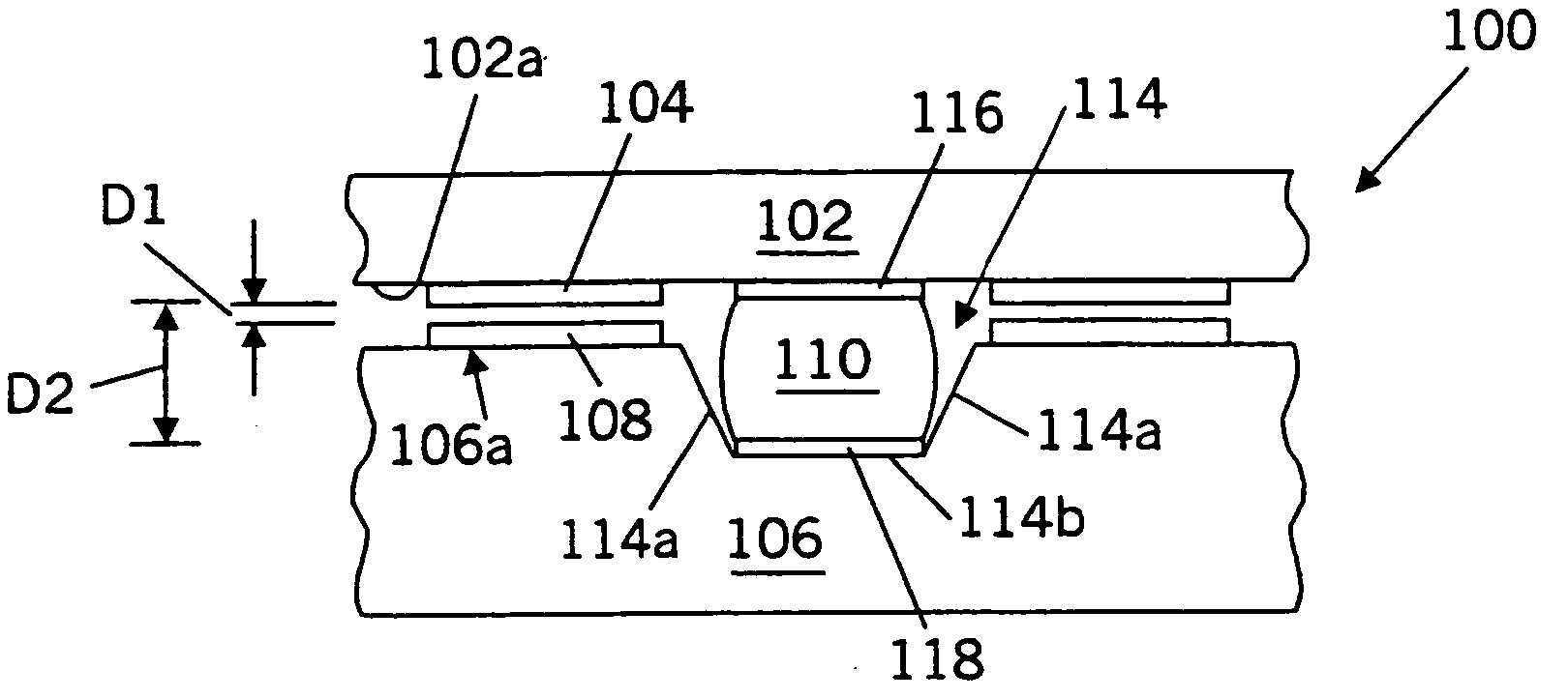
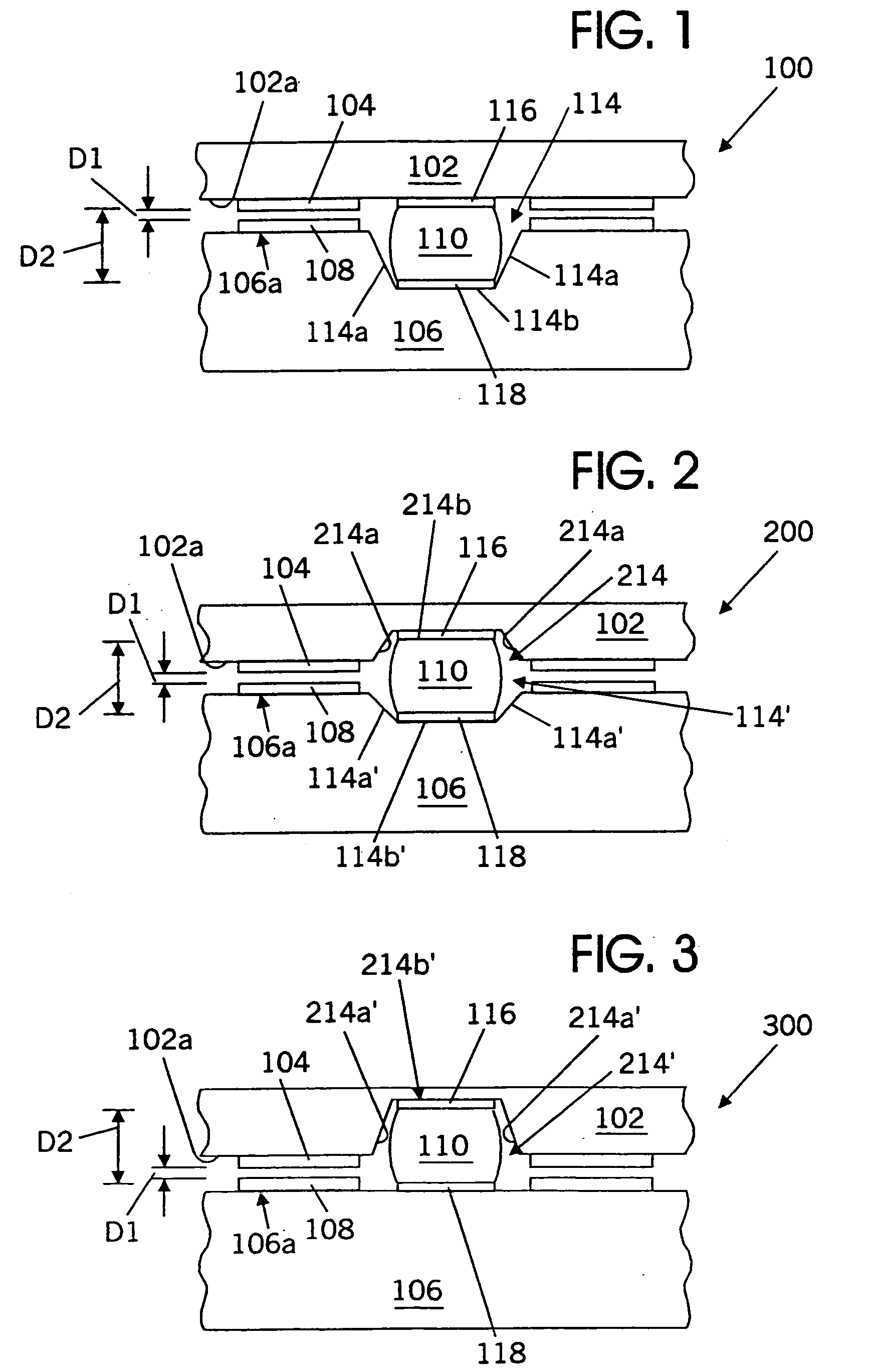
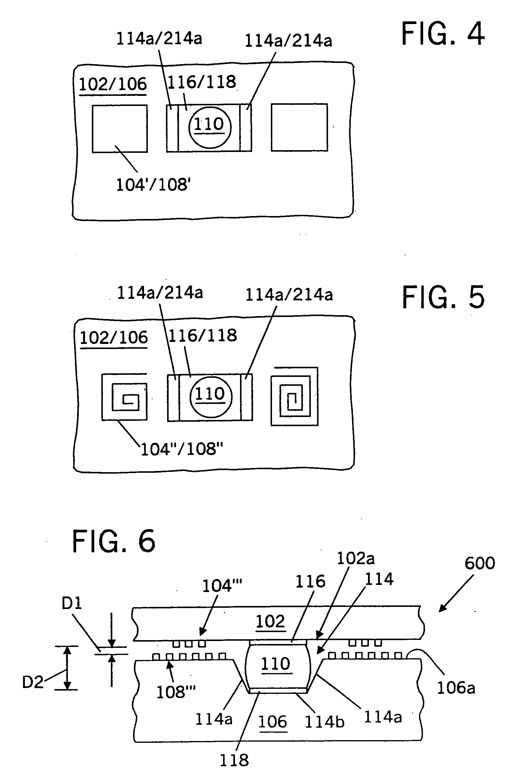
[0017] The present invention now will be described more fully hereinafter with reference to the accompanying drawings, in which preferred embodiments of the invention are shown. This invention may, however, be embodied in many different forms and should not be construed as limited to the embodiments set forth herein. Rather, these embodiments are provided so that this disclosure will be thorough and complete, and will fully convey the scope of the invention to those skilled in the art. In the drawings, the thickness of layers and regions are exaggerated for clarity. Like numbers refer to like elements throughout. It will be understood that when an element such as a layer, region or substrate is referred to as being “on” another element, it can be directly on the other element or intervening elements may also be present. In contrast, when an element is referred to as being “directly on” another element, there are no intervening elements present. It will also be understood that when a...


PUM


Abstract

Microelectronic packages include a first microelectronic substrate having a first face and a first AC-coupled interconnect element on the first face. A second microelectronic substrate includes a second face and a second AC-coupled interconnect element on the second face. A buried solder bump extends between the first and second faces, and is at least partially buried beneath the first and / or second faces, to maintain the first and second AC-coupled interconnect elements in closely spaced apart relation. The buried solder bump also may couple DC power between the first and second substrates. Other technologies also may be used to maintain the AC-coupled interconnect elements in closely spaced apart relation and to couple DC power between the substrates. The first and second AC-coupled interconnect elements may be first and second capacitor plates, first and second inductors and / or first and second combined inductive and capacitive elements.

Description

FIELD OF THE INVENTION [0001] This invention relates to microelectronic devices, and more particularly to microelectronic packages for microelectronic devices. BACKGROUND OF THE INVENTION [0002] Microelectronic devices, such as integrated circuit chips, are widely used in consumer and commercial applications. As the integration density of microelectronic devices continues to increase, it may become increasingly difficult to provide a sufficient quantity of high performance interconnects that connect the microelectronic device to a next level package. The interconnects may be used to transfer signals and / or power. Accordingly, the interconnect density and / or performance may be a limiting factor in the further integration of microelectronic devices. [0003] It is known to provide Alternating Current (AC)-coupled interconnects for microelectronic devices. These AC-coupled interconnects may be characterized by the absence of a Direct Current (DC) connection. Instead, AC-coupled interconn...

Claims


Application Information

Patent Timeline
Patent Type & Authority Applications(United States)
IPC IPC(8): H01L23/13H01L23/48H01L23/498H05K1/02H05K1/16H05K3/34
CPCH01L23/13H01L2225/06531H01L23/49816H01L23/5223H01L23/5227H01L23/642H01L23/645H01L24/73H01L25/0657H01L2224/16H01L2225/06513H01L2225/06593H01L2924/01013H01L2924/01078H01L2924/01082H01L2924/14H01L2924/19041H01L2924/19103H01L2924/30107H01L2924/3011H05K1/0239H05K1/0243H05K1/0263H05K1/165H05K3/3436H05K2201/09036H05K2201/09472H05K2201/10727H01L2924/01006H01L2924/01023H01L2924/01033H01L2924/01322H01L23/48H01L2224/05568H01L2224/05573H01L2924/00014H01L2224/05599
Inventor FRANZON, PAUL D.MICK, STEPHEN E.WILSON, JOHN M.
Owner NORTH CAROLINA STATE UNIV
Why Eureka
Try Eureka