Probe apparatus assembly and method

a technology of probe apparatus and assembly method, which is applied in the direction of instruments, measurement devices, connections, etc., can solve the problems of not being able to extend to 50 microns or less, their individual components become increasingly small, and are incompatible with many modern devices

Inactive Publication Date: 2011-08-25
GLOBALFOUNDRIES INC
View PDF23 Cites 0 Cited by
  • Summary
  • Abstract
  • Description
  • Claims
  • Application Information

AI Technical Summary

Benefits of technology

[0007]In accordance with another aspect of the invention, a probe apparatus is provided and includes a probe layer formed with two or more through-holes, conductors, independently electrically coupled to test equipment, disposed on and insulated from a sidewall of each of the through-holes, a probe disposed within each of the through-holes, each probe being spaced from the corresponding conductor and thereby movable upon application of external forces thereto and a compliant layer connected to each of the probes and sufficiently compliant to independently allow each of the probes to at least temporarily contact each of the corresponding conductors upon the respective application of the external forces to the probes
[0008]In accordance with another aspect of the invention, a probe apparatus is provided and includes a compliant layer to support two or more probes within corresponding through-holes in a probe layer such that the probes are spaced from conductors disposed on respective through-hole sidewalls and thereby movable upon application of external forces thereto, the support of the two or more probes being achieved with sufficient compliance to independently allow each of the probes to at least temporarily contact the corresponding conductors upon the respective application of the external forces thereto.

Problems solved by technology

As electronic devices become increasingly small, their individual components become increasingly small as well.
Current test probe technologies, however, do not typically extend to pitches of 50 microns or less and, thus, are often incompatible with many modern devices.
Rigid interposers have been proposed as a solution to this problem, but relatively small and non-compliant solder balls and the lack of flatness in the devices being tested make it unclear if this approach can be successful.
Currently, the proposed solutions to these problems involve temporarily soldering on the “loopback” but, in practice, this does not appear to be effective.

Method used


Image

  • Probe apparatus assembly and method
  • Probe apparatus assembly and method
  • Probe apparatus assembly and method

Examples


Embodiment Construction

[0016]The use of through-silicon-vias (TSV) and other micro-electro-mechanical system (MEMS) technologies makes possible a microplunger testing probe apparatus for use with a device having a desired and, in many cases, small (e.g., less than 50 microns) device contact pitch that is also relatively compliant. This type of structure could be attached to a test board for both regular testing functions and loopback functionality and could be incorporated into a socket for product application to thereby allow the device to be removed and reinserted without reflow.

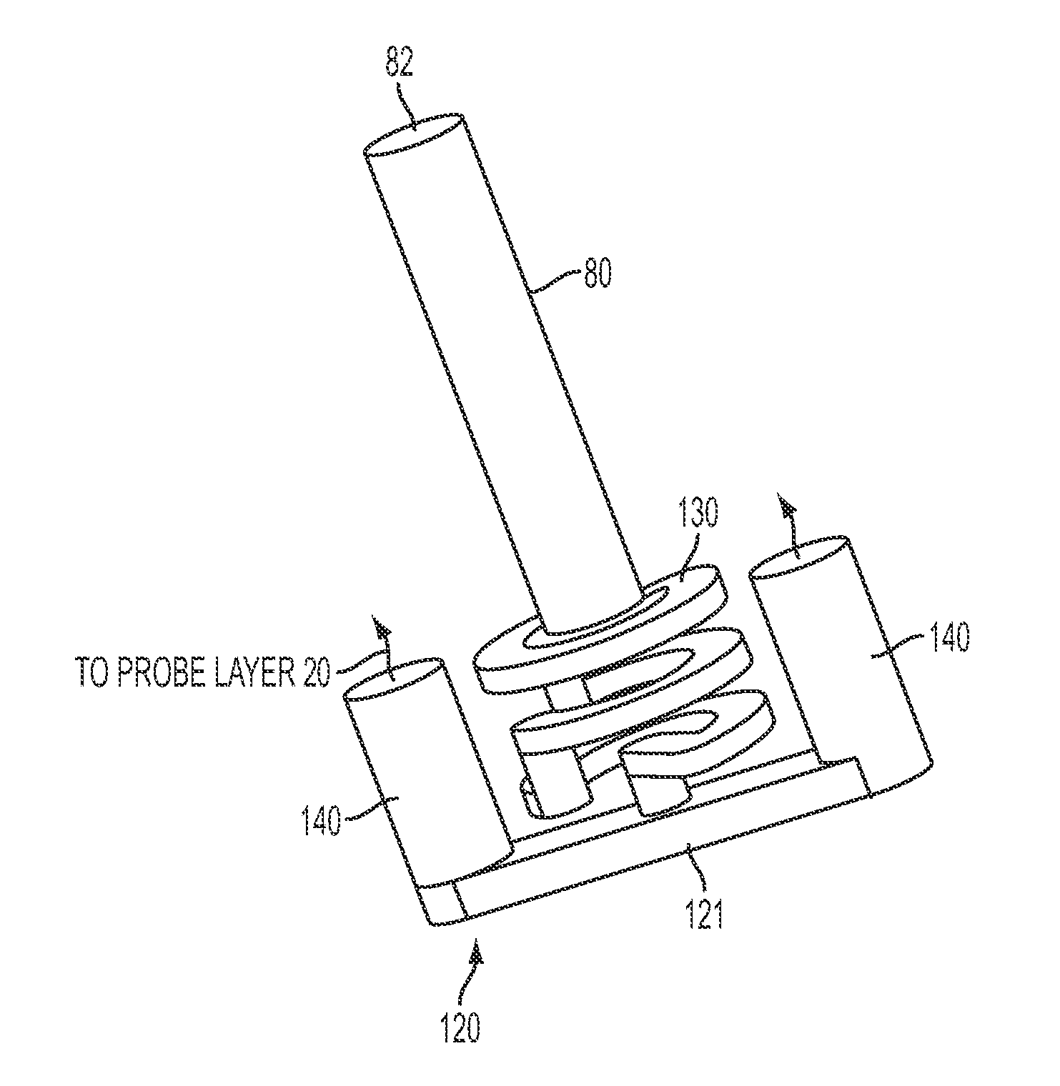
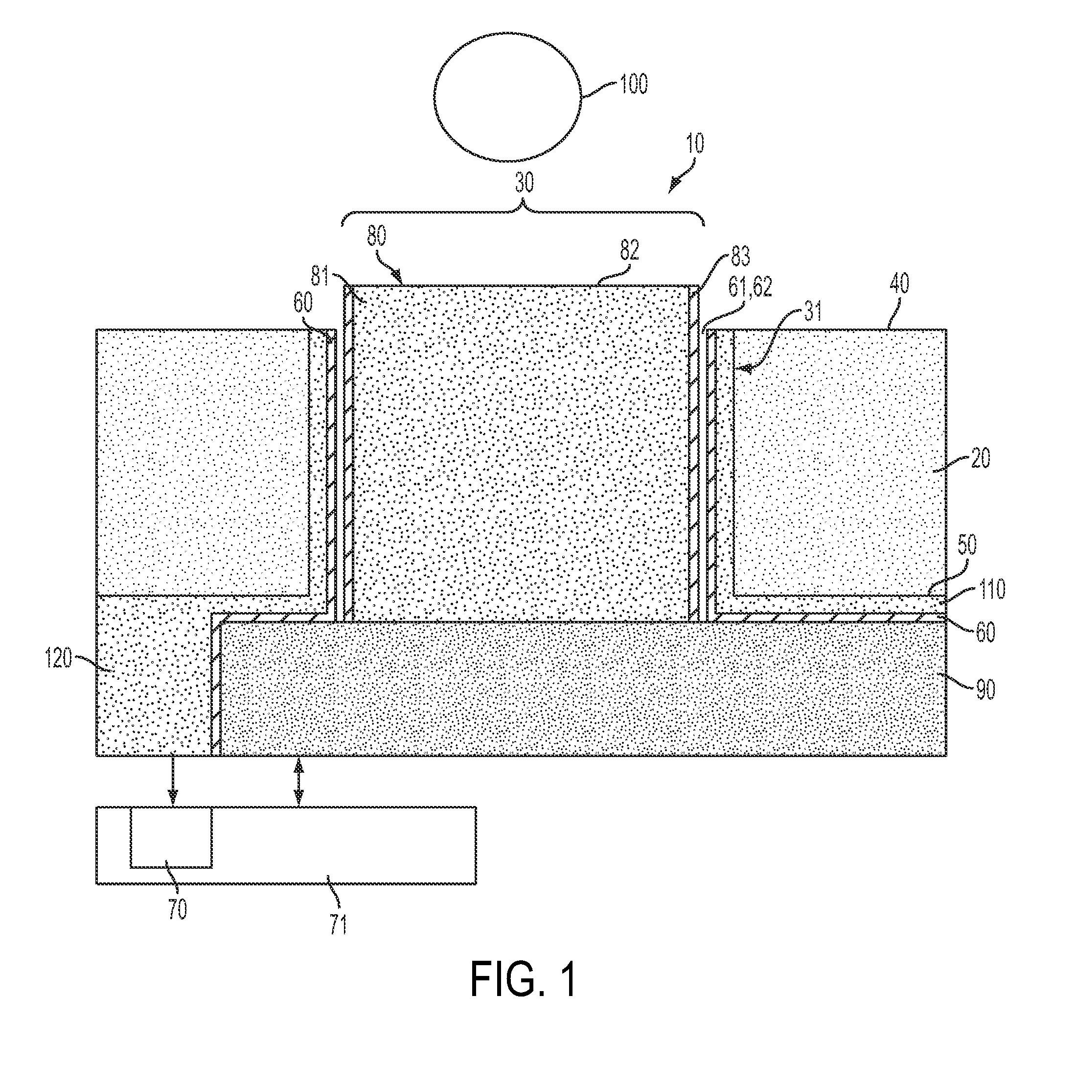
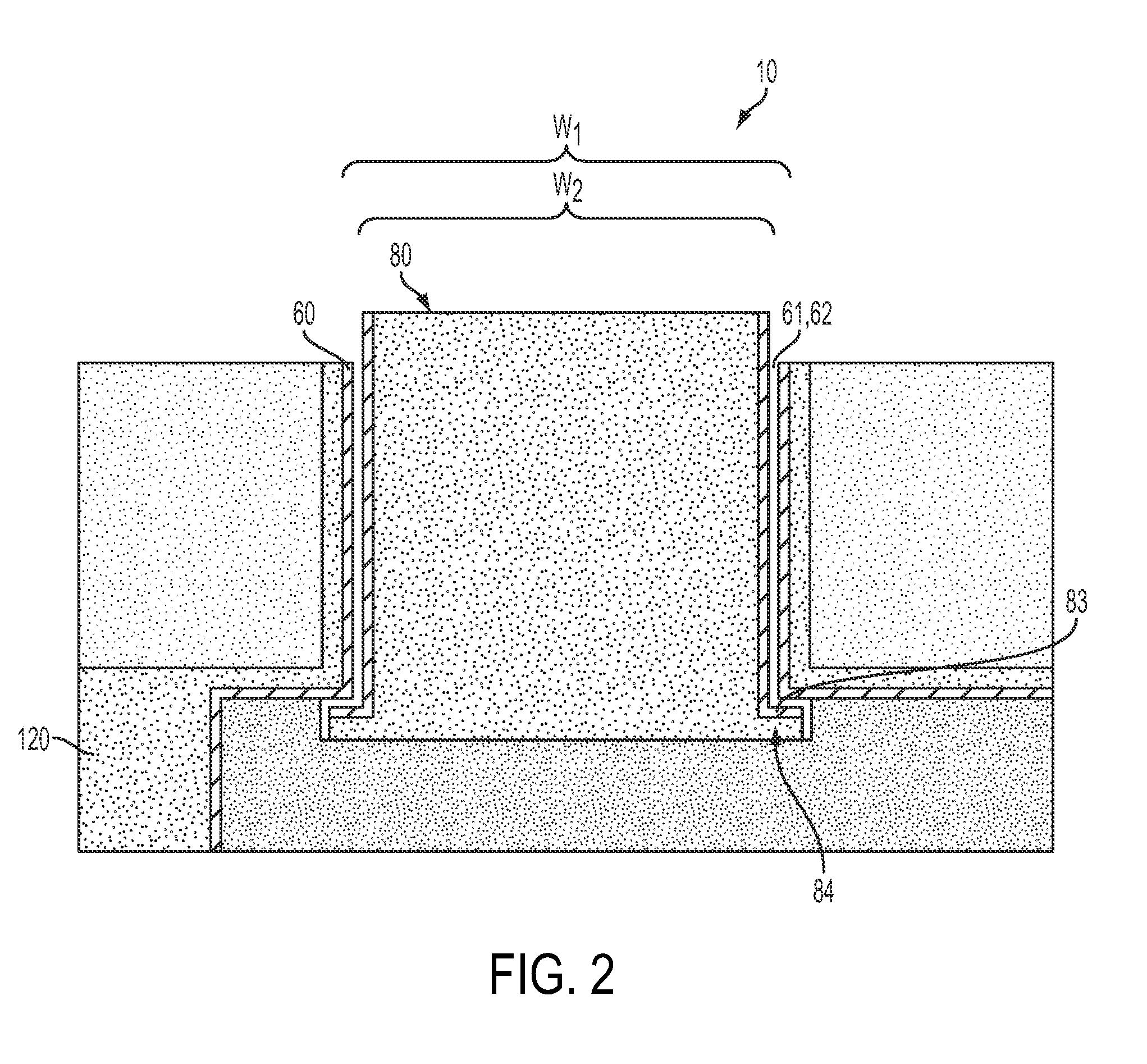
[0017]With reference to FIG. 1, a probe apparatus 10 is provided and includes a probe layer 20 formed with a through-hole 30 extending between first and second opposing surfaces 40 and 50. A conductor 60 is disposed on and insulated from a sidewall 31 of the through-hole 30. The conductor 60 is electrically coupled to test equipment 70 mounted on a substrate 71. A probe 80 is disposed within the through-hole 30 to be normally sp...


PUM

PropertyMeasurementUnit
external forceaaaaaaaaaa
conductiveaaaaaaaaaa
elastomericaaaaaaaaaa

Abstract

A probe apparatus is provided and includes a probe layer formed with a through-hole, a conductor, electrically coupled to test equipment, disposed on and insulated from a through-hole sidewall, a probe disposed within the through-hole to be spaced from the conductor and thereby movable upon application of an external force thereto and a compliant layer connected to the probe and sufficiently compliant to allow the probe to at least temporarily contact the conductor upon the application of the external force thereto.

Description

BACKGROUND[0001]Aspects of the present invention are directed to a probe apparatus, a method of assembling a probe apparatus and a method of operating a probe apparatus.[0002]As electronic devices become increasingly small, their individual components become increasingly small as well. Device contact pitches, therefore, particularly in the areas of silicon carriers and other 3D technologies, continue to tighten and are, in many cases, on a scale of less than 50 microns. Current test probe technologies, however, do not typically extend to pitches of 50 microns or less and, thus, are often incompatible with many modern devices.[0003]Rigid interposers have been proposed as a solution to this problem, but relatively small and non-compliant solder balls and the lack of flatness in the devices being tested make it unclear if this approach can be successful. Similar concerns apply to testing of carriers that require a “loopback” function to be tested. Currently, the proposed solutions to t...

Claims


Application Information

Patent Timeline
Patent Type & Authority Applications(United States)
IPC IPC(8): G01R31/02H01R43/00
CPCG01R1/06716Y10T29/49224G01R1/06744
Inventor SCHULTZ, MARK D.
Owner GLOBALFOUNDRIES INC
Why Eureka
Try Eureka