Semiconductor integrated circuit

Inactive Publication Date: 2010-02-04
RENESAS ELECTRONICS CORP
View PDF8 Cites 11 Cited by
  • Summary
  • Abstract
  • Description
  • Claims
  • Application Information

AI Technical Summary

Benefits of technology

[0010]That is, according to the present invention, since the power supply control circuit installed separately from the central processing unit controls the first switch in response to the first signal output by the CPU and the first switch controls source voltage supply to the functional macro, the central processing unit does not need to control the state of the functional macro unlike the conventional techniques. Consequently, the central processing unit can perform primary processes without receiving periodic interrupt signals for power supply control. Thus, the present invention can efficiently control power supply without hindering operation of the central processing unit.
[0011]The present invention can efficiently control power supply to functional macros in a semiconductor integrated circuit.

Problems solved by technology

Under such conditions, more time is required to complete the primary processes of the CPU, resulting in increased power consumption.
Consequently, the technique described in Japanese Patent Laid-Open No. 2004-192296 has a technical problem to be solved: namely, the semiconductor integrated circuit cannot control power supply efficiently.

Method used


Image

  • Semiconductor integrated circuit
  • Semiconductor integrated circuit
  • Semiconductor integrated circuit

Examples


first embodiment

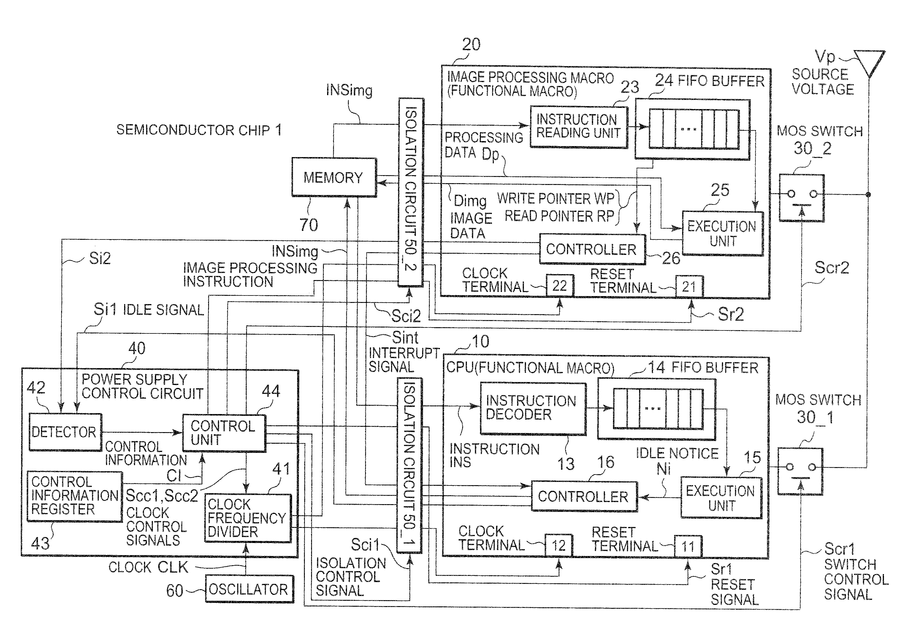
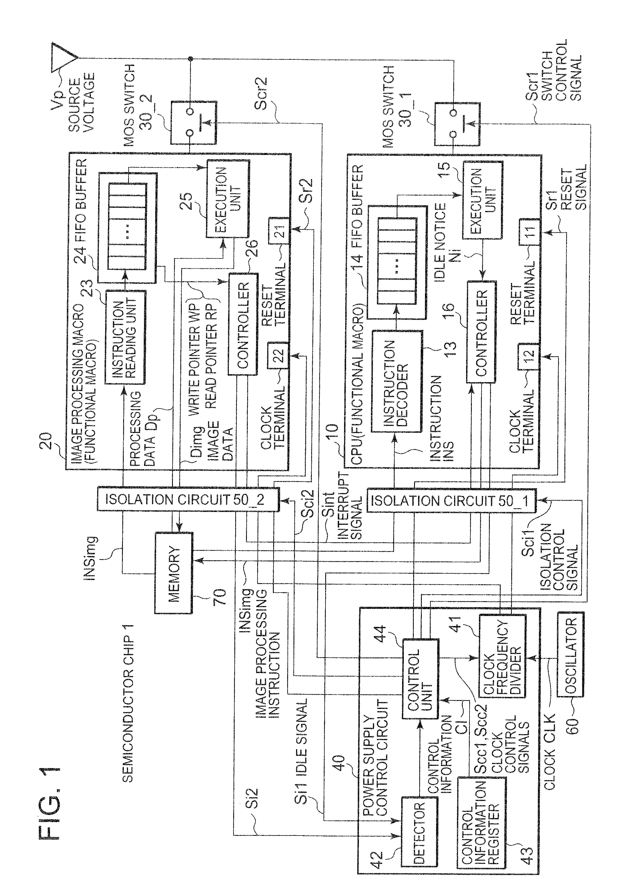
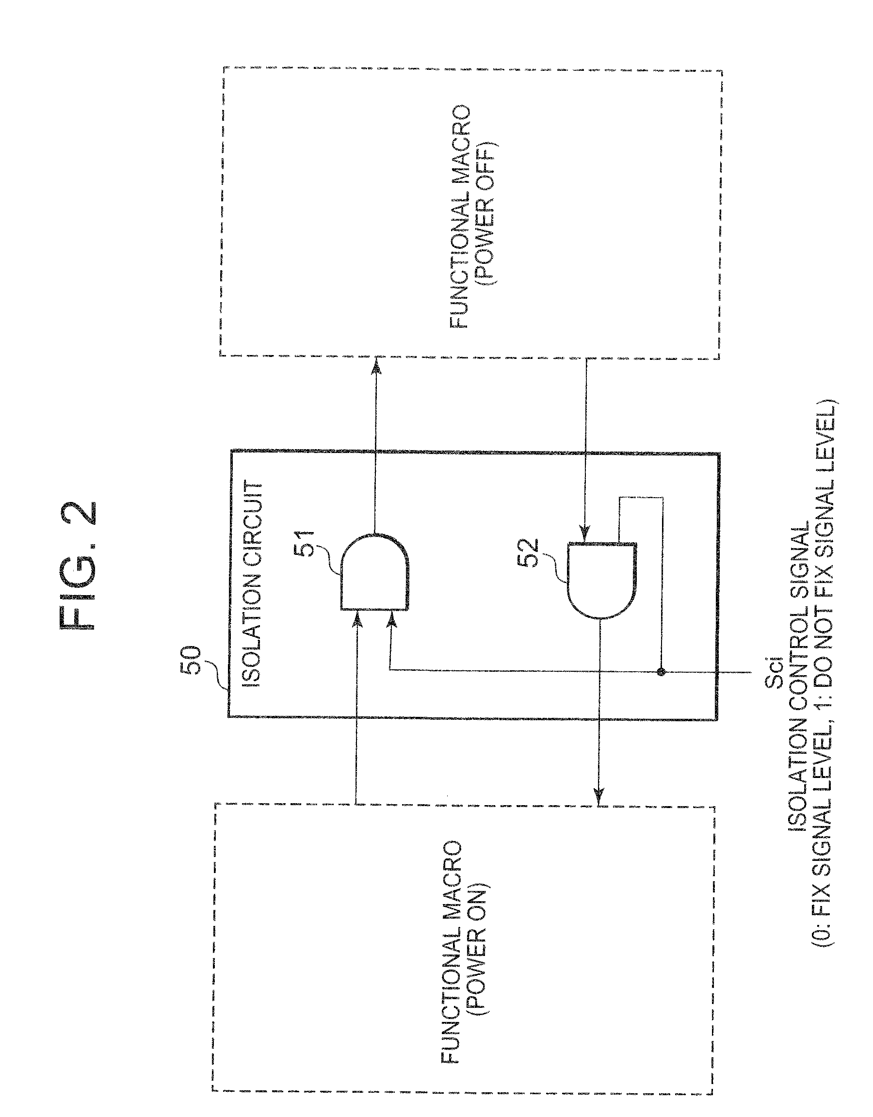
[0022]The semiconductor chip 1 according to the present embodiment shown in FIG. 1 includes a CPU (Central Processing Unit) 10 and image processing macro 20, first and second switches such as MOS (Metal Oxide Semiconductor) switches 30_1 and 30_2, and a power supply control circuit 40, where the CPU 10 and image processing macro 20 are examples of functional macros and the power supply control circuit 40 is hardware installed separately from the CPU 10. The first and second switches perform switching to supply or shut off a source voltage Vp to the CPU 10 and image processing macro 20, respectively. In response to idle signals Si1 and Si2 which represent idle states of the CPU 10 and image processing macro 20, respectively, the power supply control circuit 40 generates reset signals Sr1 and Sr2 which permit (order) the CPU 10 and image processing macro 20 to be reset, respectively, as well as generates control signals Scs1 and Scs2 for the MOS switches 30_1 and 30_2, respectively. I...

second embodiment

[0057]A semiconductor chip 1a according to the present embodiment shown in FIG. 5 differs from the semiconductor chip 1 according to the first embodiment in that MOS switches 30_13 to 30_16 and isolation circuits 50_13 to 50_16 are provided, respectively, for the components 13 to 16 of the CPU 10 and that a power supply control circuit 40a is provided to perform control over the MOS switches 30_13 to 30_16 and isolation circuits 50_1 to 50_2 as well as to perform the same control as the power supply control circuit 40 shown in FIG. 1. The present embodiment solves the problems with Japanese Patent Laid-Open No. 2004-192296 (described above): namely, the problems of a load change in source voltage caused by a sudden stop of power supply and a fall in the source voltage resulting from an inrush current produced at the start of power supply.

[0058]Also, the semiconductor chip 1a includes a CPU 10 and image processing macro 20 as in the case of the first embodiment.

[0059]Also, the power ...


PUM


Abstract

The present invention provides a semiconductor integrated circuit which can reduce power consumption without hampering operation of a CPU. A power supply control circuit 40 installed separately from a CPU 10 detects a signal (e.g., an idle signal Si) from the CPU 10 installed on a semiconductor chip 1. In response to the idle signal Si, the power supply control circuit 40 controls supply of a source voltage Vp to the CPU 10 by controlling a switch element 30—1. This makes it possible to control power supply efficiently without hampering the operation of the CPU 10.

Description

BACKGROUND OF THE INVENTION[0001]1. Field of the Invention[0002]The present invention relates to a semiconductor integrated circuit and, more particularly, to a semiconductor integrated circuit which reduces power consumption of functional blocks.[0003]2. Description of the Related Art[0004]A technique related to power supply control is described in Japanese Patent Laid-Open No. 2004-192296.[0005]A power consumption control circuit described in Japanese Patent Laid-Open No. 2004-192296 generally controls power supply to a functional macro—stops power supply or changes supply voltage—according to the internal state of the functional macro. Specifically, the power consumption control circuit receives, from the functional macro, a signal which represents the internal state of the functional macro. When the signal indicates an idle state, the power consumption control circuit stops power supply to the functional macro. When the signal indicates a memory access state or the like, the pow...

Claims


Application Information

Patent Timeline
IPC IPC(8): G05F1/10
CPCY02B60/1282Y02B60/32Y02B60/1278G06F1/3287G06F1/3228Y02D10/00Y02D30/50G06F1/24G06F1/26G06F1/32
Inventor SATOU, MIYUKI
Owner RENESAS ELECTRONICS CORP
Why Eureka
Try Eureka