Supercharge Your Innovation With Domain-Expert AI Agents!

High signal level compliant input/output circuits

Inactive Publication Date: 2010-02-04
QUALCOMM INC
View PDF53 Cites 13 Cited by
  • Summary
  • Abstract
  • Description
  • Claims
  • Application Information

AI Technical Summary

Benefits of technology

[0010]This application discloses a level shifter having at least one of either a pull up or a pull down circuit. The circuit is made of electronic components with reliability limits less than a maximum signal level output by the level shifter. The level shifter also has a timing circuit coupled to at least on of either the pull up or pull down circuit. The timing circuit controls a time of application of an input signal to at least one of either the pull up or pull down circuit preventing a terminal to terminal signal level experienced by the electronic components exceeding the reliability limits.
[0011]This application also discloses a level shifter having level shifting circuitry to selectively level shift an input signal to a first signal level and a second signal level depending on a mode of operation. The first signal level is less than the second signal level. The electronic components have reliability limits less than the second signal level. The level shifter also has a timing circuit coupled to the level shifting circuitry to control a time of application of an input signal to the level shifting circuitry preventing a terminal to terminal signal level experienced by the electronic components from exceeding the reliability limits.
[0012]This application also discloses a method including providing level shifting circuitry to selectively level shift an input signal to a first signal level and a second signal level depending on mode of operation. The first signal level is less than the second signal level, and the electronic components have reliability limits less than the second signal level. The method also includes coupling a timing circuit to the level shifting circuitry and adapting the timing circuitry to control a time of application of an input signal to level shifting circuitry. This prevents a terminal to terminal signal level experienced by the electronic components from exceeding the reliability limit.

Problems solved by technology

Although the foregoing example may not initially appear to be a large difference in signal level, electronic components may experience reliability (the capability of the component to operate without degraded performance over a long period of time) issues if designed for a lower signal level, such as 1.8V, and operated with a higher signal level, such as 2.6V or 3.0V.
The reliability of individual electronic components, such as transistors, can be compromised in many ways, such as electrical stress caused by prolonged application of electric fields across the terminals of the transistor.
From this table, it can readily be appreciated that operation of such electronic components using signal levels of 2.6V or 3.0V are likely to present reliability issues.
The technique for accommodating peripherals having different signal levels shown in FIG. 1 presents issues with respect to size and cost.
Moreover, costs associated with added components are incurred in the illustrated technique.
However, the use of circuitry designed for higher signal levels is generally not energy efficient and also degrades performance.
Specifically, utilizing electronic components which are designed to accommodate higher signal levels in processing lower signal levels generally consumes more energy than utilizing appropriately designed electronic components.
Thus, utilizing input / output circuitry designed to accommodate higher signal levels when processing lower signal levels, although typically not providing reliability issues, results in undesired power consumption.

Method used


Image

  • High signal level compliant input/output circuits
  • High signal level compliant input/output circuits
  • High signal level compliant input/output circuits

Examples


Embodiment Construction

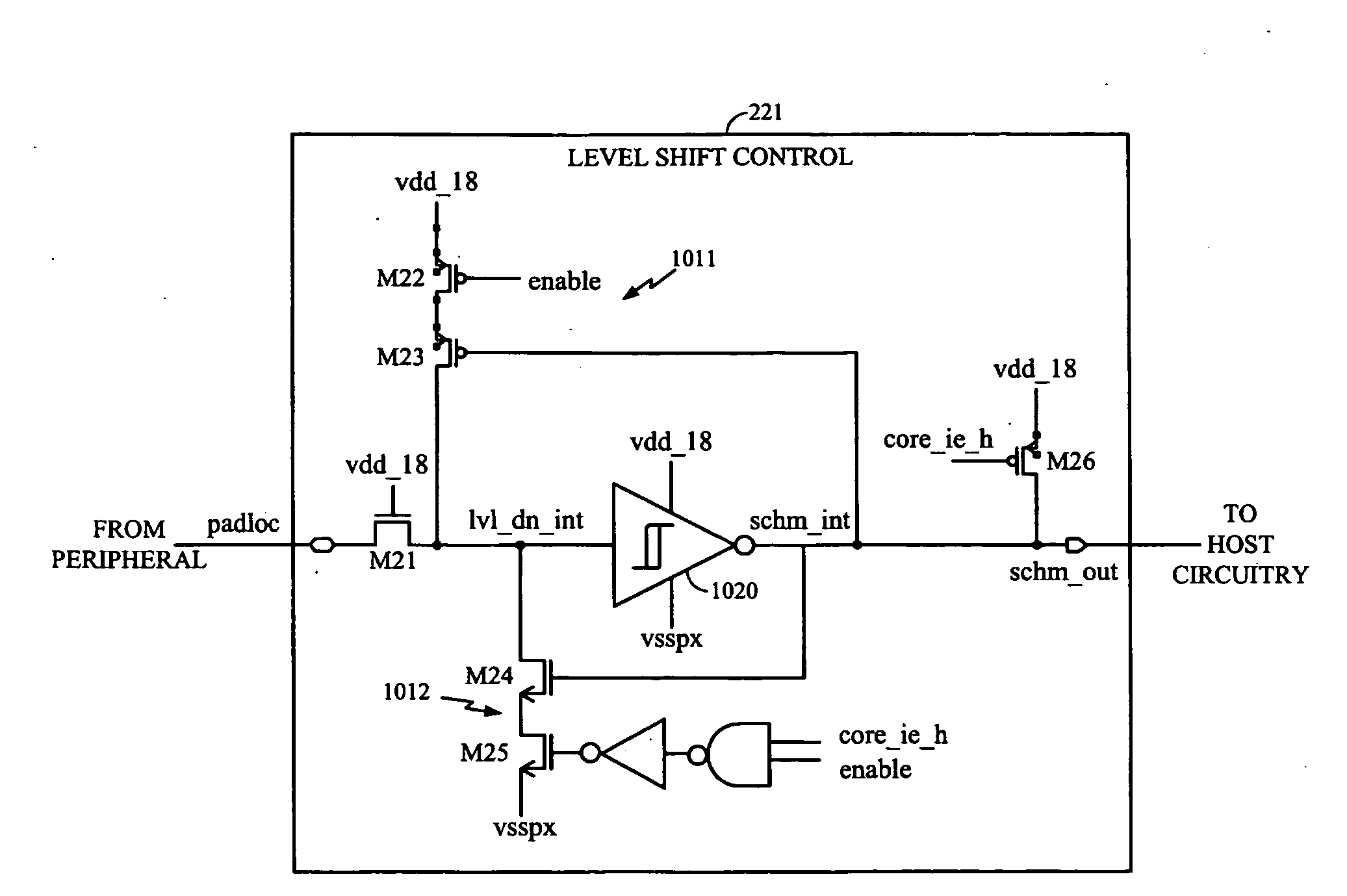
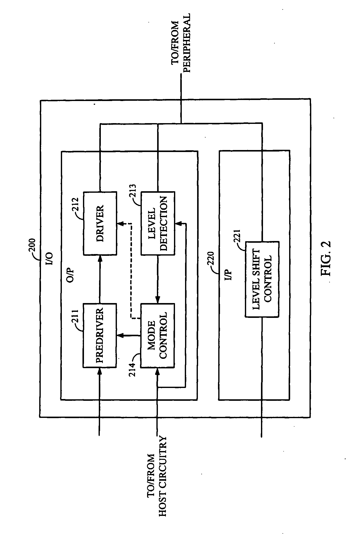
[0025]FIG. 2 shows a high level block diagram of an embodiment of high signal level compliant input / output circuitry according to the concepts herein. Input / output circuit 200 of FIG. 2 is adapted to provide interfacing between host circuitry (not shown) of a host electronic device, such as a personal computer system, personal digital assistant (PDA), cellular telephone, pager, digital sound recorder, digital camera, digital video camera, personal entertainment player, gaming device, etc., and a peripheral, such as a memory device, a display, a printer, an electronic pointer, a transducer, etc. In particular, input / output circuit 200 is adapted to accommodate peripheral interface signals of both high level (e.g., 2.6V and / or 3.0V) and of low level (e.g., 1.8V). In accommodating high signal levels, input / output circuit 200 utilizes electronic components designed for use with respect to the low signal levels. Embodiments thereby provide efficiencies with respect to size and power cons...


PUM


Abstract

A level shifter has at least one of either a pull up or a pull down circuit. The circuit is made of electronic components with reliability limits less than a maximum signal level output by the level shifter. The level shifter also has a timing circuit coupled to at least on of either the pull up or pull down circuit. The timing circuit controls a time of application of an input signal to at least one of either the pull up or pull down circuit preventing a terminal to terminal signal level experienced by the electronic components exceeding the reliability limits.

Description

CROSS-REFERENCE TO RELATED APPLICATIONS[0001]This application is related to the following U.S. patent applications, filed concurrently herewith: “HIGH SIGNAL LEVEL COMPLIANT INPUT / OUTPUT CIRCUITS” (Qualcomm reference no. 072123-A); “HIGH SIGNAL LEVEL COMPLIANT INPUT / OUTPUT CIRCUITS” (Qualcomm reference no. 072123-B); “HIGH SIGNAL LEVEL COMPLIANT INPUT / OUTPUT CIRCUITS” (Qualcomm reference no. 072123-D); “HIGH SIGNAL LEVEL COMPLIANT INPUT / OUTPUT CIRCUITS” (Qualcomm reference no. 072123-E); the disclosures of which are expressly incorporated by reference herein in their entireties.TECHNICAL FIELD[0002]The present disclosure relates generally to input / output circuits and, more particularly, to input / output circuits compatible with high signal levels.BACKGROUND[0003]The use of various electronic devices has become nearly ubiquitous in modern society. For example, desk top and portable electronic devices are typically used daily by office workers and professionals in performing their work...

Claims


Application Information

Patent Timeline
IPC IPC(8): H03L5/00
CPCH03K19/018507H03K19/00315G01R19/165H03K19/0185
Inventor SHANKAR, VIJAYGUPTA, ABHEEKSRINIVAS, VAISHNAVMOHAN, VIVEK
Owner QUALCOMM INC
Features
  • R&D
  • Intellectual Property
  • Life Sciences
  • Materials
  • Tech Scout
  • Unparalleled Data Quality
  • Higher Quality Content
  • 60% Fewer Hallucinations
Learn More