

Multilevel Variable Resistance Memory Cell Utilizing Crystalline Programming States
a programming state and variable resistance technology, applied in the direction of information storage, static storage, digital storage, etc., can solve the problems of multi-level phase-change operation, limited progress toward achieving a practical multi-level phase-change memory, and increasing difficulty in employing, so as to reduce the practical effect of resistance drift on performan
- Summary
- Abstract
- Description
- Claims
- Application Information
AI Technical Summary
Benefits of technology
Problems solved by technology
Method used
Image

Examples
example 1
[0076]In this example, fabrication of the memory device used to obtain the experimental results described hereinbelow is described. The device structure was a standard two-terminal design that included Ge32Sb14Te54 as the active material. Ge32Sb14Te54 is a variable resistance composition drawn from the phase-change class of materials. As explained in the following examples, Ge32Sb14Te54 can be stabilized in multiple crystalline programming states through electrical programming. The multiple crystalline programming states include a face-centered cubic phase, a hexagonal phase, and a series of crystalline phases that include a mixture of the face-centered cubic and hexagonal phases in varying proportions. Ge32Sb14Te54 can also be stabilized in an amorphous programming state and a plurality of mixed crystalline-amorphous programming states.
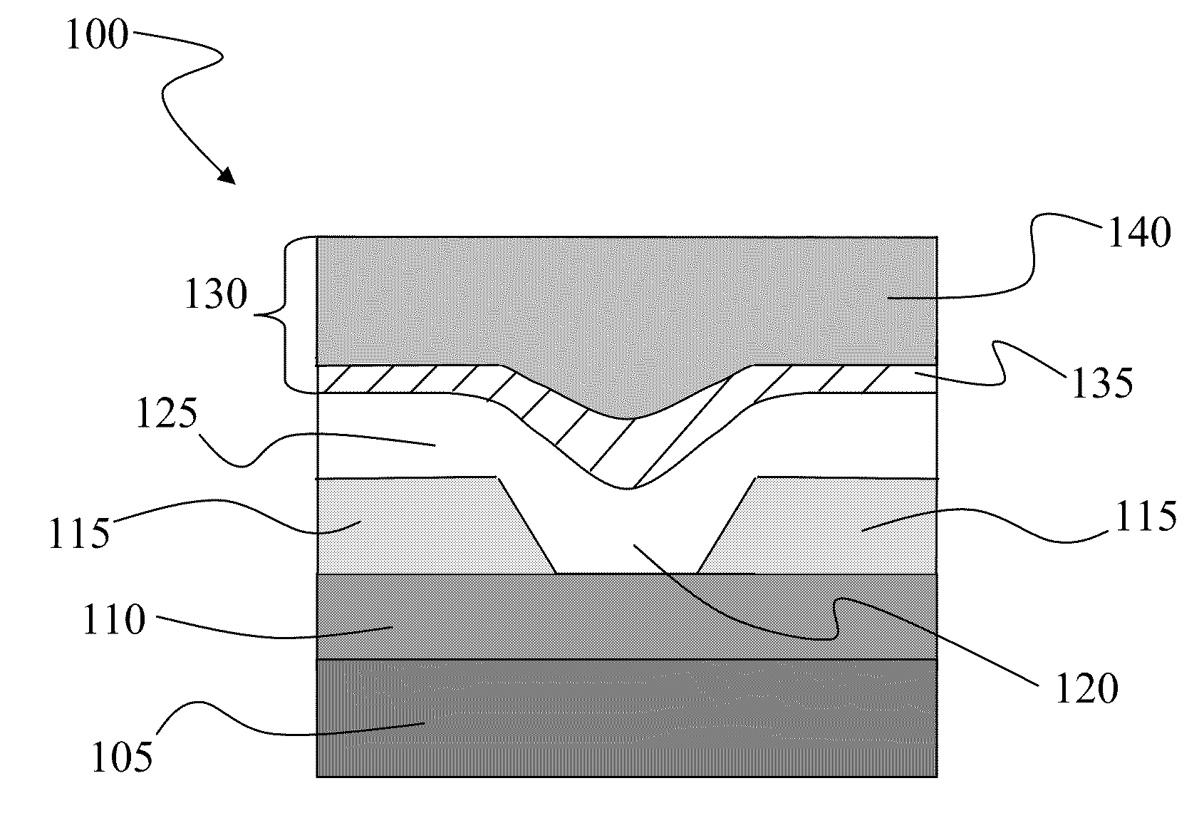
[0077]The device structure is schematically illustrated in FIG. 6. Device 100 includes substrate 105, lower electrode 110, and dielectric 115. Diele...
example 2
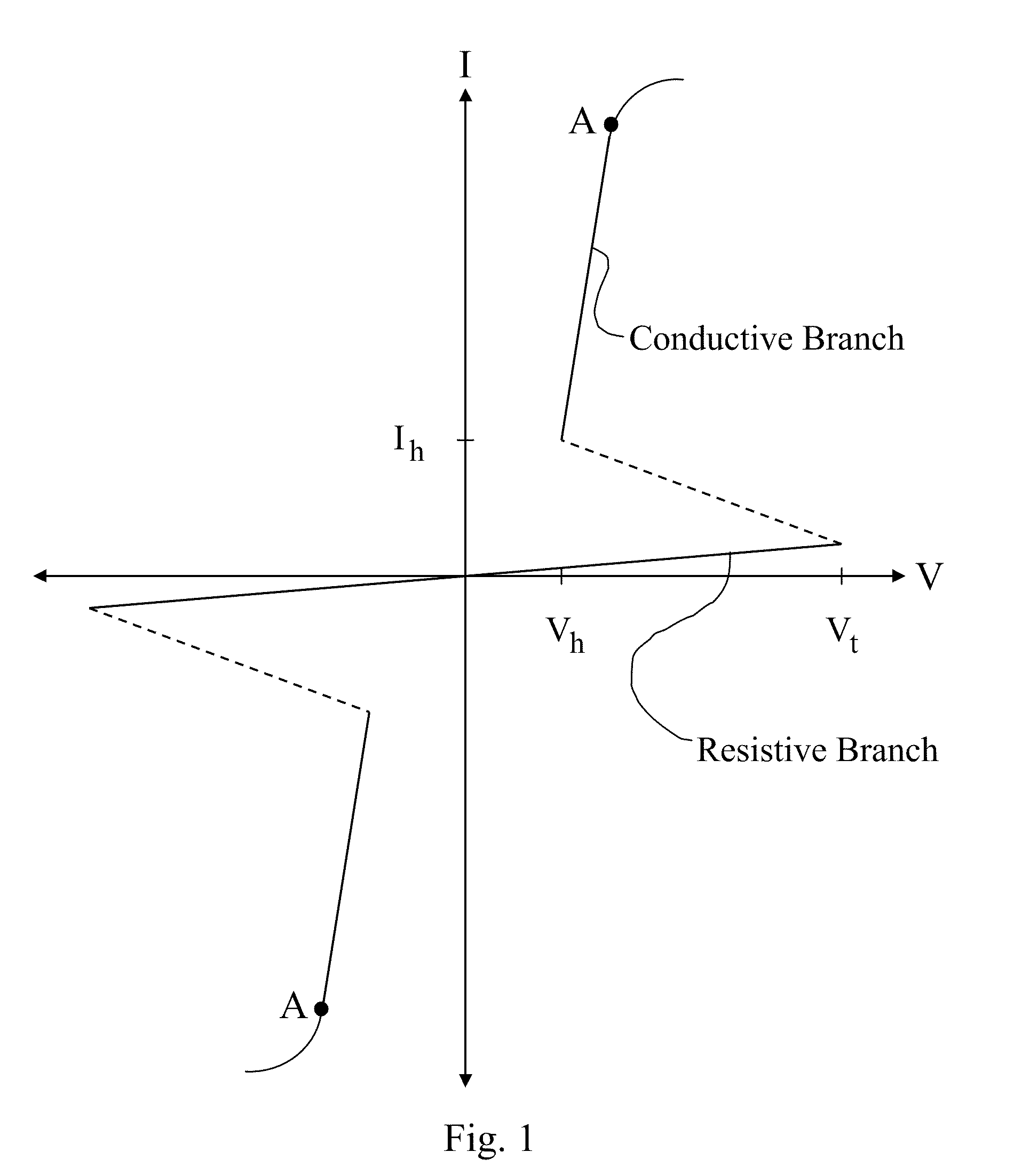
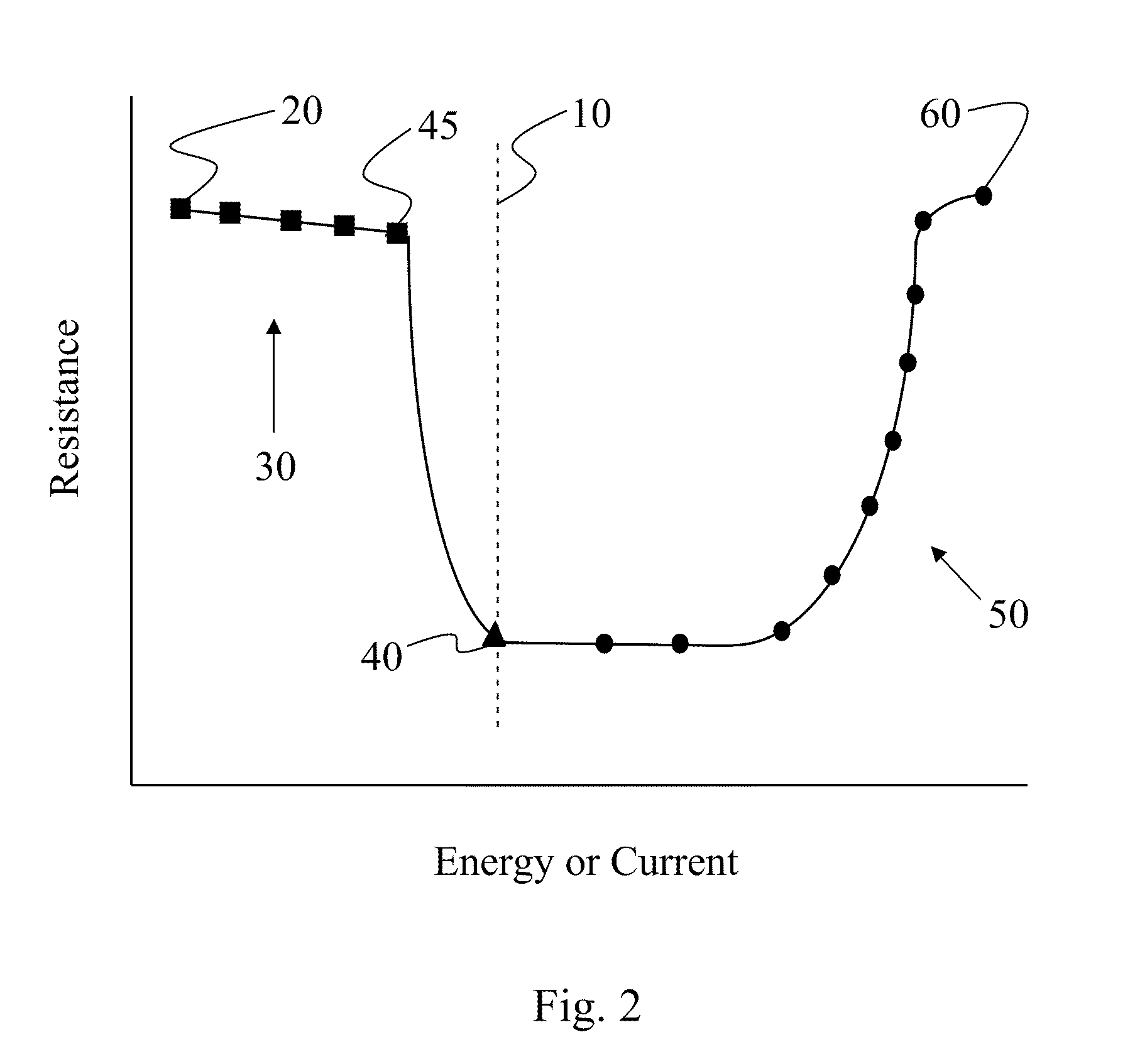
[0078]In this example, the I-V (current vs. voltage) and R-I (resistance vs. current) characteristics of the device described in Example 1 are summarized. The I-V and R-I measurements were performed by applying a series of voltage pulses of increasing amplitude between upper electrode 130 and lower electrode 110. The initial voltage pulse had an amplitude of ˜0.1 V and each successive pulse was increased in amplitude by ˜0.1-0.2V up to a maximum voltage of ˜7V. The voltage pulses had a duration of 500 ns. A fixed resistor of ˜2 Kohms was placed in series with the pulse generator to serve as a current limiter. While each voltage pulse was applied, the current passing through the device was measured. After each voltage pulse was applied, the resistance of the device was measured. In this way, a current and resistance was obtained for each voltage pulse. The points were plotted to obtain the I-V relationship shown in FIG. 7 and the R-I relationship shown in FIG. 8. The process was repe...
example 3
[0081]This example illustrates the effect of programming conditions on the resistance of the device described in Examples 1 and 2 hereinabove. More specifically, this example demonstrates that the characteristics of the electrical programming pulses can be varied to consistently stabilize a plurality of crystalline programming states. A programming experiment was completed in which the thermal environment of the phase-change material was varied through modification of the quench rate of the phase-change material.
[0082]The programming technique involved measurement of the device resistance after application of a two-pulse sequence. The first of the two pulses was a reset pulse having a voltage amplitude sufficient to melt the active phase-change material and a falltime that was sufficiently short to stabilize the phase-change device in its reset state. As noted hereinabove, the reset state is an amorphous programming state that lacks appreciable crystalline content. By decreasing the...
PUM
 Abstract
Description
Claims
Application Information