Control circuit of read operation for semiconductor memory apparatus

Active Publication Date: 2010-02-11
SK HYNIX INC
View PDF4 Cites 6 Cited by
  • Summary
  • Abstract
  • Description
  • Claims
  • Application Information

AI Technical Summary

Benefits of technology

[0027]A control circuit of a read operation can ensure an operational margin by changing a data output time interval in synchronization with a clock in accordance with the operational frequency in a read operation in a SERDES type semiconductor memory apparatus.

Problems solved by technology

However, the parallel input / output has a disadvantage in that the number of buses required for transmitting data increases and the more the data transmission distance increases, which results in an increased unit cost of the product.
As a result, a problem occurs where the data that has been transmitted to the global input / output line is not transmitted to the pipe latch 213 at the exact time.
This problem can be exacerbated in a high-frequency operation and cause the semiconductor memory apparatus to malfunction.

Method used


Image

  • Control circuit of read operation for semiconductor memory apparatus
  • Control circuit of read operation for semiconductor memory apparatus
  • Control circuit of read operation for semiconductor memory apparatus

Examples


Embodiment Construction

.”

BRIEF DESCRIPTION OF THE DRAWINGS

[0031]Features, aspects, and embodiments are described in conjunction with the attached drawings, in which:

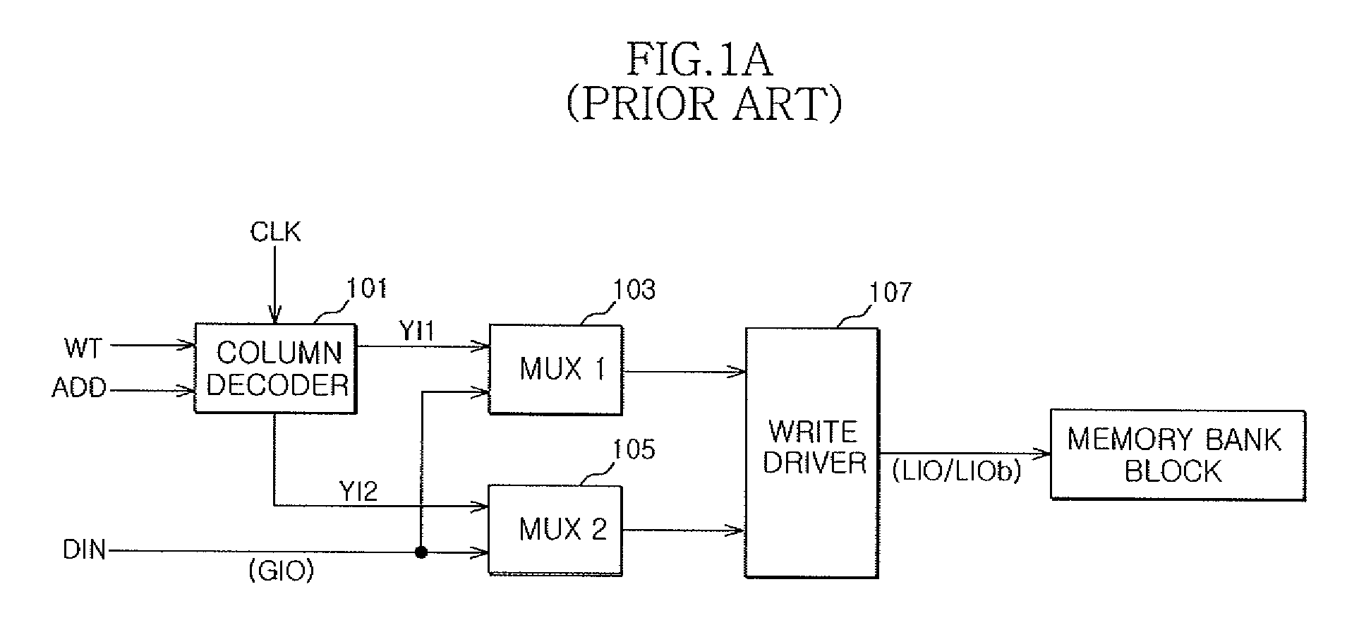
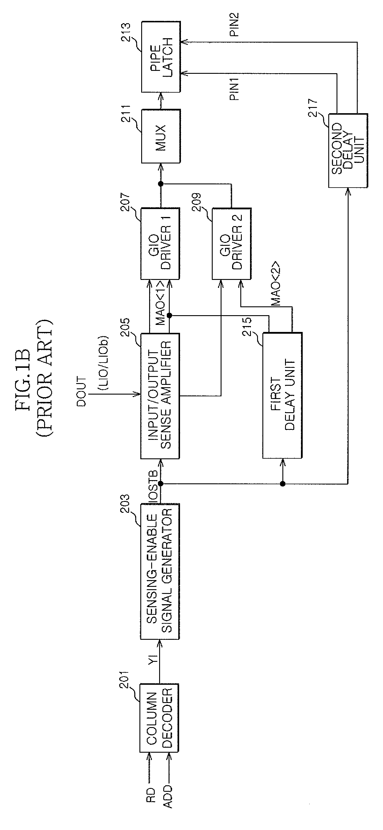
[0032]FIG. 1A and FIG. 1B are circuit diagrams showing a procedure for a command process in a conventional SERDES type semiconductor memory apparatus;

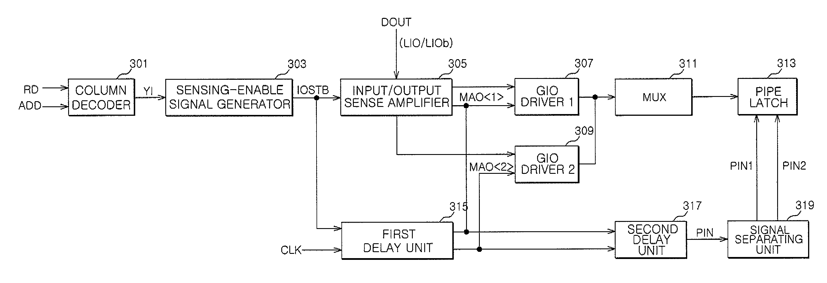
[0033]FIG. 2 is a diagram showing the configuration of a control circuit of a read operation according to an embodiment of the present invention;

[0034]FIG. 3 is a diagram showing the configuration of the first delay unit shown in FIG. 2;

[0035]FIG. 4 is a diagram showing the configuration of the second delay unit shown in FIG. 2; and

[0036]FIG. 5 is a diagram showing the configuration of a control circuit of a read operation according to another embodiment of the present invention.

DETAILED DESCRIPTION

[0037]Hereinafter, preferred embodiments of the present invention will be described in detail with reference to the accompanying drawings.

[0038]FIG. 2 is a diagram showing the configuration of a contro...


PUM


Abstract

A control circuit for a read operation of a SERDES (SERializer and DESeriallizer) type semiconductor memory apparatus is disclosed that includes a first delay unit that is configured to generate and output a first delay signal to a first global input / output line driver by receiving a sensing-enable signal ‘IOSTB’, and to generate and output a second delay signal to a second global input / output line driver by receiving the sensing-enable signal. The first delay unit generates the second delay signal by delaying the sensing-enable signal in synchronization with a clock. The semiconductor memory apparatus also includes a second delay unit configured to generate a pipe latch control signal in response to the first delay signal and the second delay signal.

Description

CROSS-REFERENCES TO RELATED PATENT APPLICATION[0001]The present application claims priority under 35 U.S.C 119(a) to Korean Application No. 10-2008-0077692, filed on Aug. 8, 2008, in the Korean Intellectual Property Office, which is incorporated herein by reference in its entirety as set forth in full.BACKGROUND[0002]1. Technical Field[0003]The present invention described herein generally relates to a semiconductor memory apparatus, and more particularly, to a control circuit of a read operation for a semiconductor memory apparatus.[0004]2. Related Art[0005]Typical semiconductor memory apparatuses use a parallel input / output system for exchanging data with an external chipset using a single port having a plurality of input / output pins. The parallel input / output has an advantage of processing data at a high speed since the parallel input / output can simultaneously transmit several bits of data.[0006]However, the parallel input / output has a disadvantage in that the number of buses requ...

Claims


Application Information

Patent Timeline
IPC IPC(8): H03L7/00
CPCG11C7/1039G11C7/1051G11C7/1066G11C7/222G11C7/1078G11C7/1096G11C7/22G11C7/1069G11C7/10G11C8/00
Inventor KIM, KWI DONG
Owner SK HYNIX INC
Why Eureka
Try Eureka