Full Wafer Width Scanning Using Steps and Scan System

a scanning system and wafer technology, applied in the direction of optics, instruments, photomechanical equipment, etc., can solve the problems of obscuring the purpose, requiring a significant overhead of time, and requiring the use of reticles, so as to avoid obscuring the purpose

Inactive Publication Date: 2010-02-11
ASML HLDG NV
View PDF7 Cites 15 Cited by
  • Summary
  • Abstract
  • Description
  • Claims
  • Application Information

AI Technical Summary

Benefits of technology

[0012]This section is for the purpose of summarizing some aspects of the present invention and to briefly introduce some preferred embodiments. Simplifications or omissions may be made to avoid obscuring the purpose of the section. Such simplifications or omissions are not intended to limit the scope of the present invention.

Problems solved by technology

Reticles, and the use of reticles, can be expensive, especially for small wafer runs.
A step and scan lithographic system requires that the reticle stage and wafer stage change scan direction for each exposure field This changing of direction requires a significant overhead of time for the reticle and wafer stages to ramp up to speed, ramp down from speed, and change scan direction.

Method used


Image

  • Full Wafer Width Scanning Using Steps and Scan System
  • Full Wafer Width Scanning Using Steps and Scan System
  • Full Wafer Width Scanning Using Steps and Scan System

Examples


Embodiment Construction

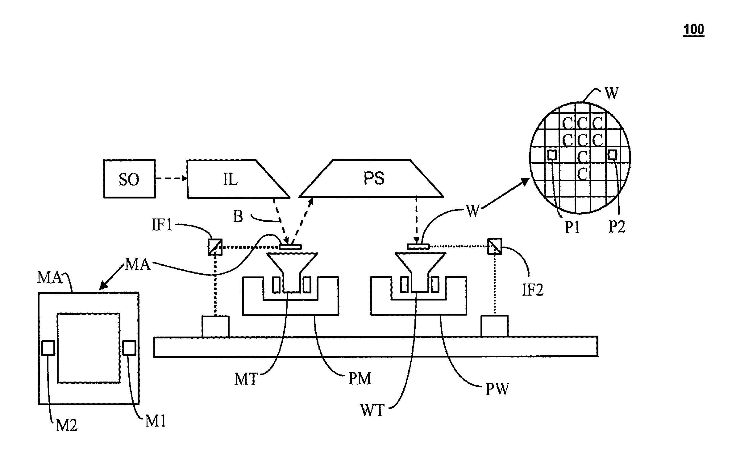
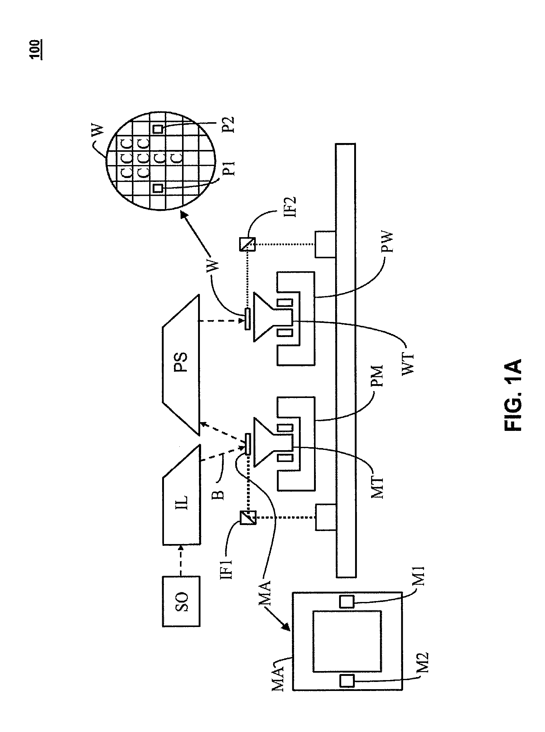
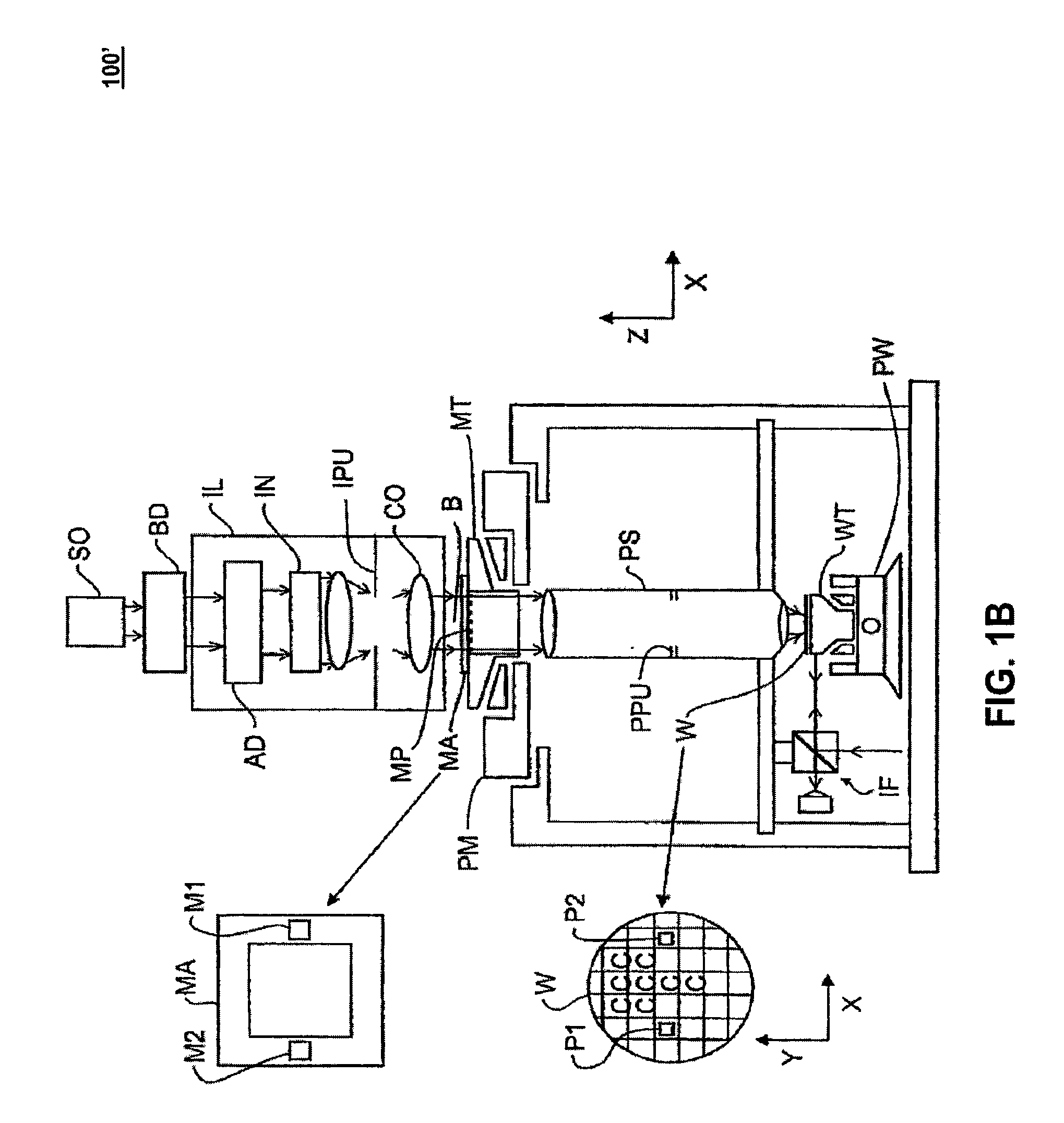
[0028]The invention will be better understood from the following descriptions of various “embodiments” of the invention. Thus, specific “embodiments” are views of the invention, but each does not itself represent the whole invention. In many cases individual elements from one particular embodiment may be substituted for different elements in another embodiment carrying out a similar or corresponding function. The present invention relates to

[0029]The embodiment(s) described, and references in the specification to “one embodiment,”“an embodiment,”“an example embodiment,” etc., indicate that the embodiment(s) described can include a particular feature, structure, or characteristic, but every embodiment cannot necessarily include the particular feature, structure, or characteristic. Moreover, such phrases are not necessarily referring to the same embodiment. Further, when a particular feature, structure, or characteristic is described in connection with an embodiment, it is understood ...


PUM


Abstract

A system and method are provided for writing a pattern onto a substrate. A patterned beam of radiation is produced using a reticle and projected onto a substrate to expose the pattern. Reticle and substrate speeds are controlled such that respective scanning speeds of the reticle and the substrate allow the pattern to be exposed across an entire width of the substrate in the scanning direction, which provides a substantial increase in wafer throughput.

Description

CROSS REFERENCE TO RELATED APPLICATIONS[0001]This application claims the benefit under 35 U.S.C. §119(e) to Provisional Patent Application No. 61 / 086,347 filed Aug. 5, 2008, which is incorporated by reference herein in its entirety.BACKGROUND[0002]1. Field of the Invention[0003]The present invention relates to a lithographic apparatus and device manufacturing method.[0004]2. Related Art[0005]A lithographic apparatus is a machine that applies a desired pattern onto a substrate, usually onto a target portion of the substrate. A lithographic apparatus can be used, for example, in the manufacture of integrated circuits (ICs), memory chips, flat panel displays, etc. In that instance, a patterning device, which is alternatively referred to as a mask or a reticle, may be used to generate a pattern to be formed on an individual layer of the IC. This pattern can be transferred onto a target portion (e.g., including part of, one, or several dies) on a substrate (e.g., a silicon wafer). Transf...

Claims


Application Information

Patent Timeline
Patent Type & Authority Applications(United States)
IPC IPC(8): G03B27/42G03B27/32
CPCG03F7/70358G03F7/70466G03F7/70433G03F7/70716G03F7/70775
Inventor SEWELL, HARRY
Owner ASML HLDG NV
Why Eureka
Try Eureka