Circuit board, electro-optic device, and electronic apparatus

Active Publication Date: 2010-02-11
E INK CORPORATION
View PDF1 Cites 14 Cited by
  • Summary
  • Abstract
  • Description
  • Claims
  • Application Information

AI Technical Summary

Benefits of technology

[0006]An advantage of some aspects of the invention is that a circuit

Problems solved by technology

Formation of small contact holes requires high

Method used


Image

  • Circuit board, electro-optic device, and electronic apparatus
  • Circuit board, electro-optic device, and electronic apparatus
  • Circuit board, electro-optic device, and electronic apparatus

Examples


Embodiment Construction

[0026]Embodiments of the invention will now be described in detail with reference to the drawings. In the description below, an electrophoretic device is described as one example of an electro-optic device. One example of an electronic apparatus that includes the electrophoretic device in a display unit will also be described.

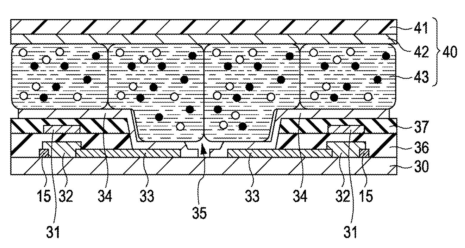
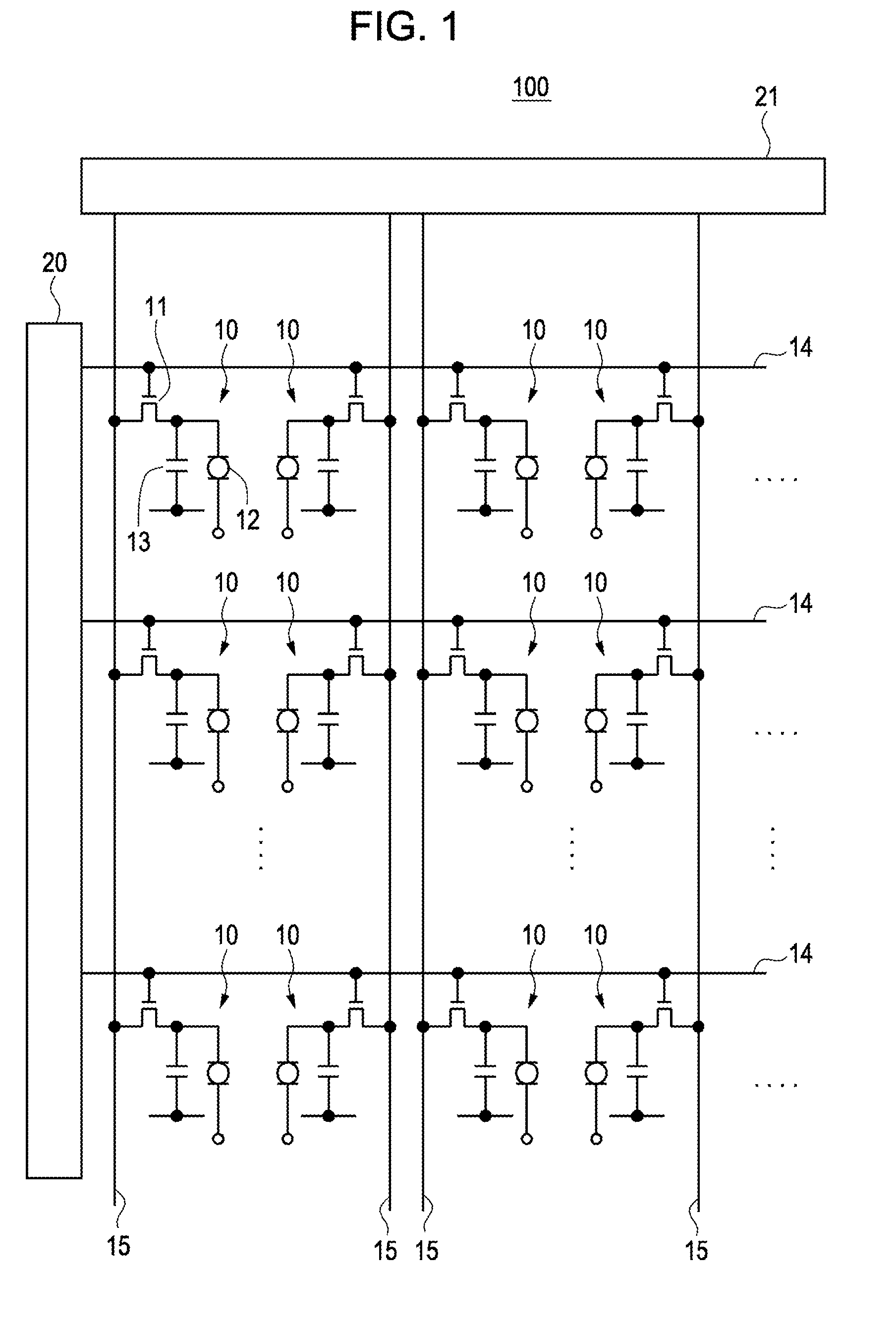
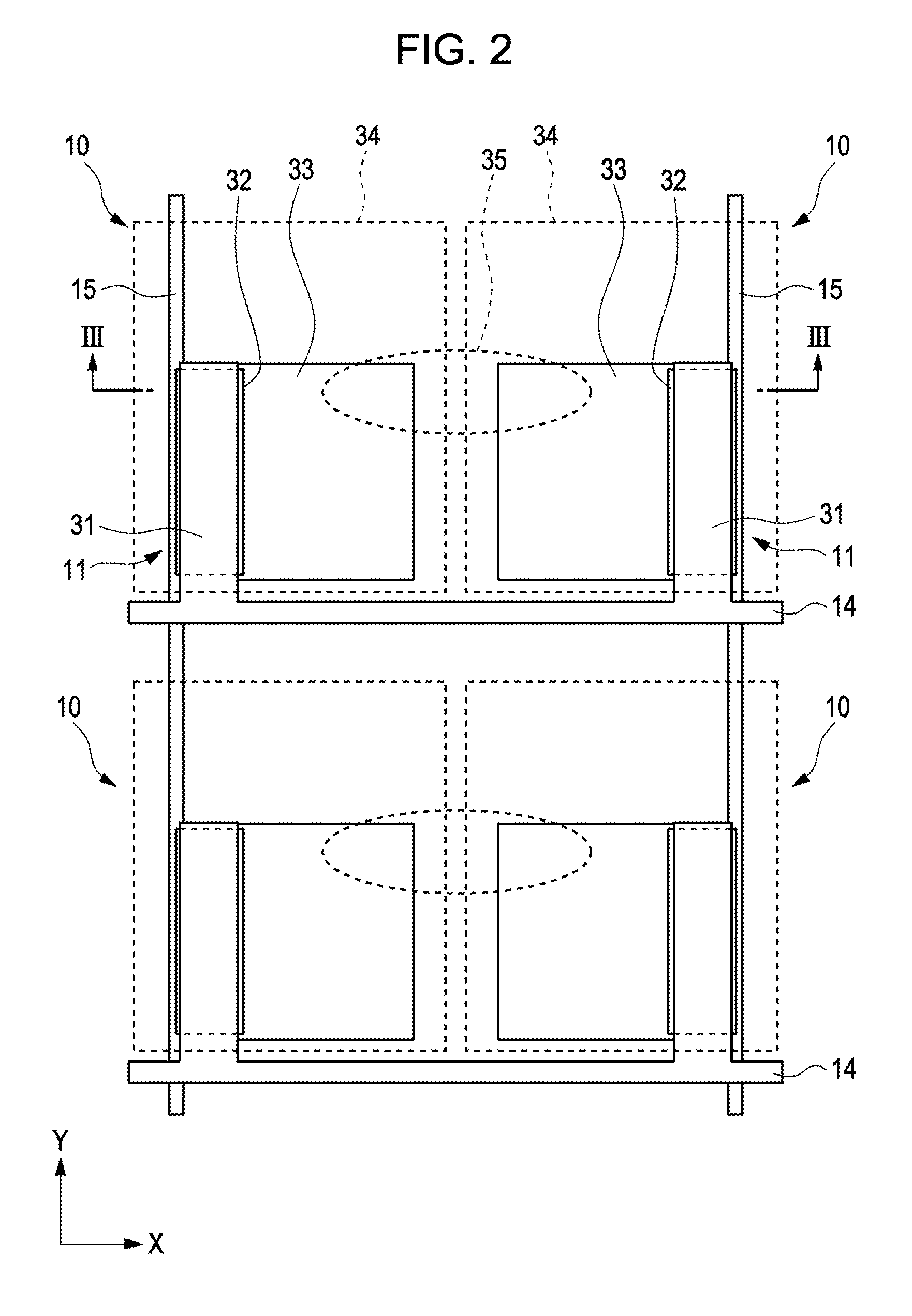
[0027]FIG. 1 is a diagram showing a circuit configuration of an electrophoretic device according to one embodiment. An electrophoretic device (electrophoretic panel) 100 shown in FIG. 1 is formed on a substrate, such as a glass substrate or a plastic substrate, and includes a plurality of pixel units 10 arranged into a matrix. Each pixel unit 10 includes a transistor 11, an electrophoretic element 12, and a capacitor element 13. Such a configuration of the pixel unit 10 is only exemplary. Other configurations, such as one not including the capacitor element 13, may also be employed.

[0028]The transistors 11 are respectively disposed at intersections of a plurali...


PUM


Abstract

A circuit board includes a substrate; a plurality of scan lines disposed on the substrate, the scan lines extending in a first direction; a plurality of signal lines disposed on the substrate, the signal lines extending in a second direction intersecting the first direction; a plurality of transistors, each of which is electrically connected to corresponding one of the plurality of scan lines and corresponding one of the plurality of signal lines; an insulating layer that covers the plurality of scan lines, the plurality of signal lines, and the plurality of transistors; and a plurality of electrodes, each of which is electrically connected to corresponding one of the plurality of transistors. One opening is formed in the insulating layer for every electrode group, the electrode group being constituted by at least two adjacent electrodes among the plurality of electrodes, and each of the plurality of electrodes is electrically connected to the corresponding one of the transistors through the opening.

Description

BACKGROUND[0001]1. Technical Field[0002]The present invention relates to a circuit board suited for use in electro-optic devices, such as electrophoretic devices and liquid crystal devices, and other devices, an electro-optic device including the circuit board, and an electronic apparatus including the circuit board or the electro-optic device.[0003]2. Related Art[0004]An electro-optic device, such as a liquid crystal device and an electrophoretic device used for display applications and the like, or a detecting device such as a fingerprint sensor includes a circuit board (active matrix substrate) that has a plurality of electrodes arranged in a two-dimensional pattern and a plurality of transistors corresponding to the respective electrodes. A typical procedure for manufacturing such a circuit board is as follows. First, a plurality of transistors are formed on a substrate, and then an insulating film (insulating layer) is formed on the transistors. Contact holes (through holes or ...

Claims


Application Information

Patent Timeline
IPC IPC(8): G02F1/167H01L27/12G02F1/16756G02F1/16757
CPCG02F1/167G02F1/136227G02F1/16756G02F1/16757
Inventor AOKI, TAKASHI
Owner E INK CORPORATION
Why Eureka
Try Eureka