Semiconductor storage device, method of controlling the same, controller and information processing apparatus

a semiconductor memory and storage device technology, applied in the direction of memory adressing/allocation/relocation, instruments, digital storage, etc., can solve the problems of inability to perform high-speed address translation, limited number of blocks capable of being simultaneously updated, and inability to improve writing efficiency

Active Publication Date: 2010-02-11
KIOXIA CORP
View PDF4 Cites 133 Cited by
  • Summary
  • Abstract
  • Description
  • Claims
  • Application Information

AI Technical Summary

Benefits of technology

[0024]A semiconductor storage device according to an aspect of the present invention comprises a first memory area configured in a volatile semiconductor memory which performs writing of data by a first unit or less, the first unit being an access unit to the semiconductor storage device, second and third memory areas configured in a nonvolatile semiconductor memory which performs writing of data by a second unit and performs erasing of data by a third unit, the third unit being twice or larger natural number times as large as the second unit, and a controller executing; a fir...

Problems solved by technology

As a result, the correspondence list dose not fit in a main memory of a controller in the secondary storage device, whereby there arises a problem that the address translation cannot be performed at high speed.
However, the above technique has a problem that since the data block and the log block have one-to-one correspondences, the number of blocks capable of being simultaneously updated is limited to the number of log blocks.
Namely, when the data of a small size is written in a large number of blocks, the data reflection processing is performed in the state that there are a large number of empty pages in the log block...

Method used


Image

  • Semiconductor storage device, method of controlling the same, controller and information processing apparatus
  • Semiconductor storage device, method of controlling the same, controller and information processing apparatus
  • Semiconductor storage device, method of controlling the same, controller and information processing apparatus

Examples


example 1

(a). Operation Example 1

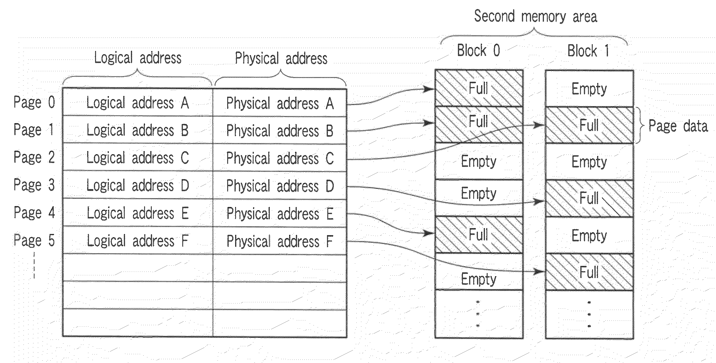
[0325]When the data Y is written in the first memory area 11 in the initial state that there is no data in the first memory area 11, as a result, only sector unit data Y (512 B) exists in the first memory area 11 over the logical address range of a size of the block unit including the data Y (the logical address range is equal to the logical address range of the data X). The controller 10 can detect the data amount by searching the cash management table.

[0326]The above size 512 B is smaller than 256 kB which is defined as the predetermined threshold value in the first condition.

[0327]The controller 10 transfers the data Y stored in the first memory area 11 to the second memory area 12 as page unit data (hereinafter referred to as data P) over the logical address range calculated by aligning the logical address of the data Y by a size of the page unit.

[0328]Since a size of the sector unit data Y is smaller than a size of the page unit, the missing data is requ...

example 2

(b). Operation Example 2

[0337]The initial state that, superseding data of 384 kB included in the logical address range calculated by aligning the logical address of the data Y by a size of the block unit (the logical address range is equal to the logical address range of the data X) has been already written in the first memory area 11, is assumed.

[0338]In this initial state, when the sector unit data Y which is included in the logical address range of the data X and not stored in the first memory area 11 is written in the first memory area 11, data of (384 kB+512 B) including the data Y exists in the logical address range of the data X. The controller 10 can detect the data amount by searching the cash management table.

[0339]The above size (384 kB+512 B) is not smaller than 256 kB which is defined as the predetermined threshold value in the first condition.

[0340]The controller 10 transfers the data of (384 kB+512 B) including the data Y, which is stored in the first memory area 11, ...

first embodiment

(1) First Embodiment

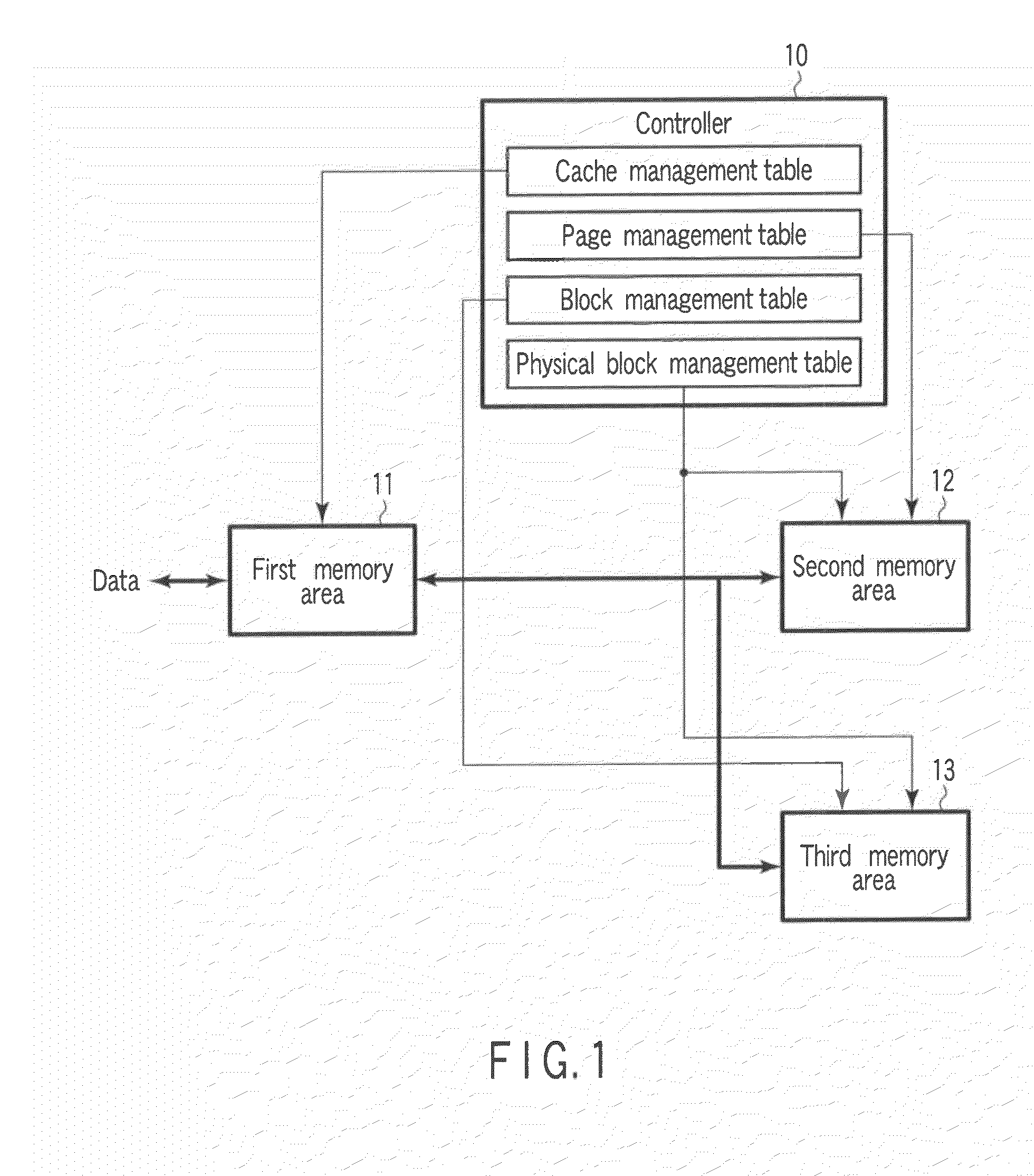
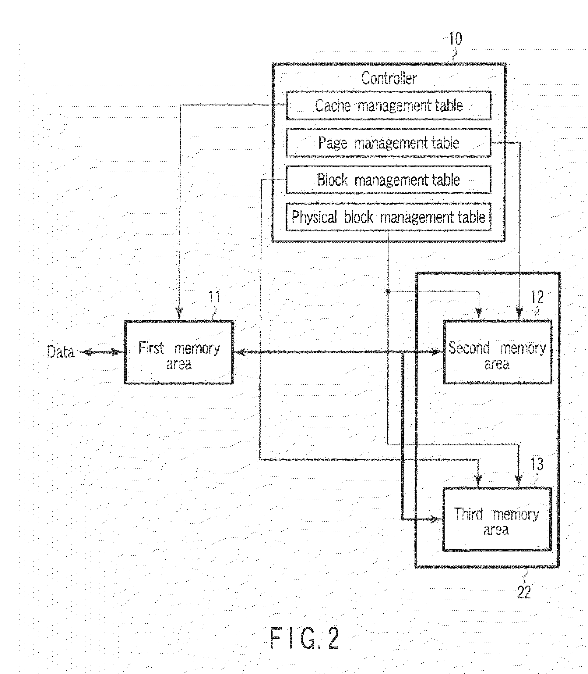
[0416]FIG. 20 shows a semiconductor storage device according to a first embodiment.

[0417]A first memory area 11 temporarily stores data from a host apparatus. The data is written by the sector unit (the first unit) or less in the first memory area 11. The first memory area 11 is configured in a volatile semiconductor memory such as a DRAM.

[0418]A second memory area 12 is composed of blocks in a nonvolatile semiconductor memory 22. In the nonvolatile semiconductor memory 22, the unit in which reading / writing is executed at one time is a page (the second unit) and the unit in which erasing is executed at one time is a block (the third unit). A size of the block unit is natural number times as large as a size of the page unit. The second memory area 12 stores data by the “small unit” which is equal to the page unit.

[0419]A third memory area 13 is composed of blocks in the nonvolatile semiconductor memory 22 and stores data by the “large unit” which is equal to the b...


PUM


Abstract

A semiconductor storage device includes a first memory area configured in a volatile semiconductor memory, second and third memory areas configured in a nonvolatile semiconductor memory, and a controller which executes following processing. The controller executes a first processing for storing a plurality of data by the first unit in the first memory area, a second processing for storing data outputted from the first memory area by a first management unit in the second memory area, and a third processing for storing data outputted from the first memory area by a second management unit in the third memory area.

Description

CROSS-REFERENCE TO RELATED APPLICATIONS[0001]This is a Continuation Application of PCT Application No. PCT / JP2008 / 073950, filed Dec. 25, 2008, which was published under PCT Article 21(2) in English.[0002]This application is based upon and claims the benefit of priority from prior Japanese Patent Applications No. 2007-339943, filed Dec. 28, 2007; and No. 2008-046227, filed Feb. 27, 2008, the entire contents of both of which are incorporated herein by reference.BACKGROUND OF THE INVENTION[0003]1. Field of the Invention[0004]The present invention relates to a semiconductor storage device with a nonvolatile semiconductor memory.[0005]2. Description of the Related Art[0006]Like a NAND type flash memory, a nonvolatile semiconductor memory has a type which, when data is stored therein, once erases data in units called a block and thereafter to perform writing, a type which performs reading and writing in units called a page, and a type in which a unit of erasing, reading, and writing is sp...

Claims


Application Information

Patent Timeline
IPC IPC(8): G06F12/00G06F12/02
CPCG06F12/0246G06F12/0804G06F12/0866G06F2212/7201G06F2212/7202G06F2212/7209G06F3/0616G06F3/064G06F3/0656G06F3/0679G06F2212/7203G06F12/02G06F12/06G06F12/08G06F3/0604G11C11/5628G06F3/0631G06F3/0658G06F3/0685
Inventor YANO, HIROKUNIKANNO, SHINICHIHIDA, TOSHIKATSUMATSUZAKI, HIDENORIKITSUNAI, KAZUYAASANO, SHIGEHIRO
Owner KIOXIA CORP
Why Eureka
Try Eureka