Stacking Integrated Circuits containing Serializer and Deserializer Blocks using Through Silicon Via

a technology of serializer and deserializer block, applied in the direction of metal working apparatus, manufacturing tools, semiconductor/solid-state device details, etc., can solve the problems of high-speed ser/des packaging, specialized area, and difficult packaging of ser/des, so as to reduce or eliminate inductance and capacitance, reduce or eliminate the effect of inductance and capacitan

Active Publication Date: 2010-03-11
BROADPAK CORP
View PDF5 Cites 235 Cited by
  • Summary
  • Abstract
  • Description
  • Claims
  • Application Information

AI Technical Summary

Benefits of technology

[0015]This invention uses techniques to enable connecting multiple chips (dice) vertically to create a compact 3D chip package. Specifically, it uses techniques that enable high speed SER/DES circuits get connected between multiple dice or from a die to external pins via Through Silicon Via (TSV) that will reduce or eliminate the inductance and capacitance associ

Problems solved by technology

IC packaging is one area that this quest is continuously challenged.
Packaging SER/DES is a very challenging and specialized area in the w

Method used


Image

  • Stacking Integrated Circuits containing Serializer and Deserializer Blocks using Through Silicon Via
  • Stacking Integrated Circuits containing Serializer and Deserializer Blocks using Through Silicon Via
  • Stacking Integrated Circuits containing Serializer and Deserializer Blocks using Through Silicon Via

Examples


Embodiment Construction

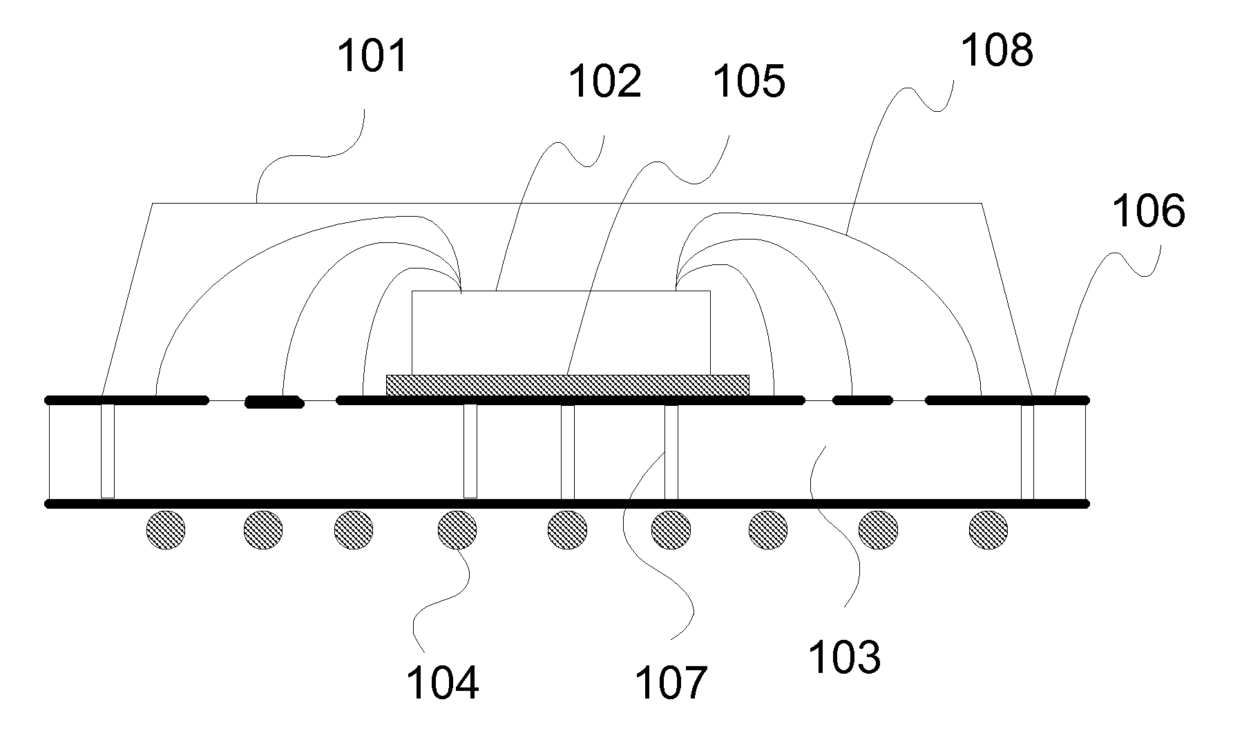
[0026]To create a more compact and space efficient integrated circuit, it is necessary to be able to stack multiple dice on top of each other. Two general methods are possible for interconnecting the stacked dice to each other and for connecting those dice to the pins or solder balls of the 3D chip package. One method is to use wirebond, meaning that to use wires to connect chips to each other or to the pins of the 3D package as shown in FIG. 3 and FIG. 4. The wirebond technique is not very useful for high speed SER / DES due to creation of inductance and capacitance.

[0027]Another technique is to use Through Silicon Via (TSV) to connect multiple stacked dice to each other or to the external pins. FIG. 8 shows an example of TSVs (801, 803) of two dice (802, 804) connected to each other. While FIG. 9 shows the contact pads (901) of one die (902) is connected to the TSVs (903) of another die (904). TSVs has so far been only used for lower speed integrated circuits. This patent extends th...


PUM

PropertyMeasurementUnit
Angleaaaaaaaaaa
Speedaaaaaaaaaa
Frequencyaaaaaaaaaa

Abstract

Methods and systems for stacking multiple chips with high speed serialiser/deserialiser blocks are presented. These methods make use of Through Silicon Via (TSV) to connect the dice to each other, and to the external pads. The methods enable efficient multilayer stacking that simplifies design and manufacturing, and at the same time, ensure high speed operation of serialiser/deserialiser blocks, using the TSVs.

Description

BACKGROUND OF THE INVENTION[0001]A Serializer / Deserializer (SER / DES) is a pair of functional blocks [integrated circuits or IC / chip] commonly used in high speed communications. These blocks convert data between serial data and parallel interfaces in each direction. Although the term “SER / DES” is generic, in speech it is sometimes used as a more pronounceable synonym for Serial Gigabit Media Independent Interface (SGMII).[0002]SER / DES chips facilitate the transmission of parallel data between two points over serial streams, reducing the number of data paths and thus, the number of connecting pins or wires required. Most SER / DES devices are capable of full duplex operation, meaning that data conversion can take place in both directions simultaneously. SER / DES chips are used in many application including Gigabit Ethernet systems, wireless network routers, fiber optic communications systems, storage applications just to name a few.[0003]Specifications and speeds vary depending on the ne...

Claims


Application Information

Patent Timeline
IPC IPC(8): H05K13/04H05K3/36
CPCH01L23/481Y10T29/53178H01L25/0657H01L2224/48227H01L2225/06513H01L2225/06517H01L2225/06527H01L2225/06541H01L2225/06572H01L2924/19041H01L24/48H01L2924/10253H01L23/66Y10T29/53174Y10T29/53183H01L2924/30107H01L2924/00H01L2924/14H01L2924/00014H01L2924/181H01L2224/32145H01L2224/48091H01L2224/73265H01L2224/45099H01L2224/45015H01L2924/207H01L2924/00012
Inventor YAZDANI, FARHANG
Owner BROADPAK CORP
Why Eureka
Try Eureka