

Contact detecting device and display device
- Summary
- Abstract
- Description
- Claims
- Application Information
AI Technical Summary
Benefits of technology
Problems solved by technology
Method used
Image

Examples
first embodiment
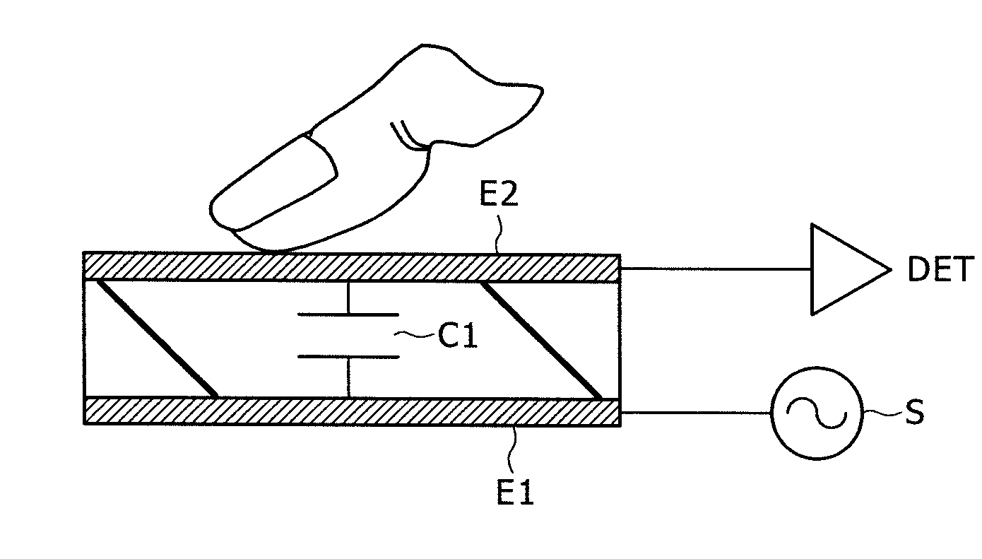
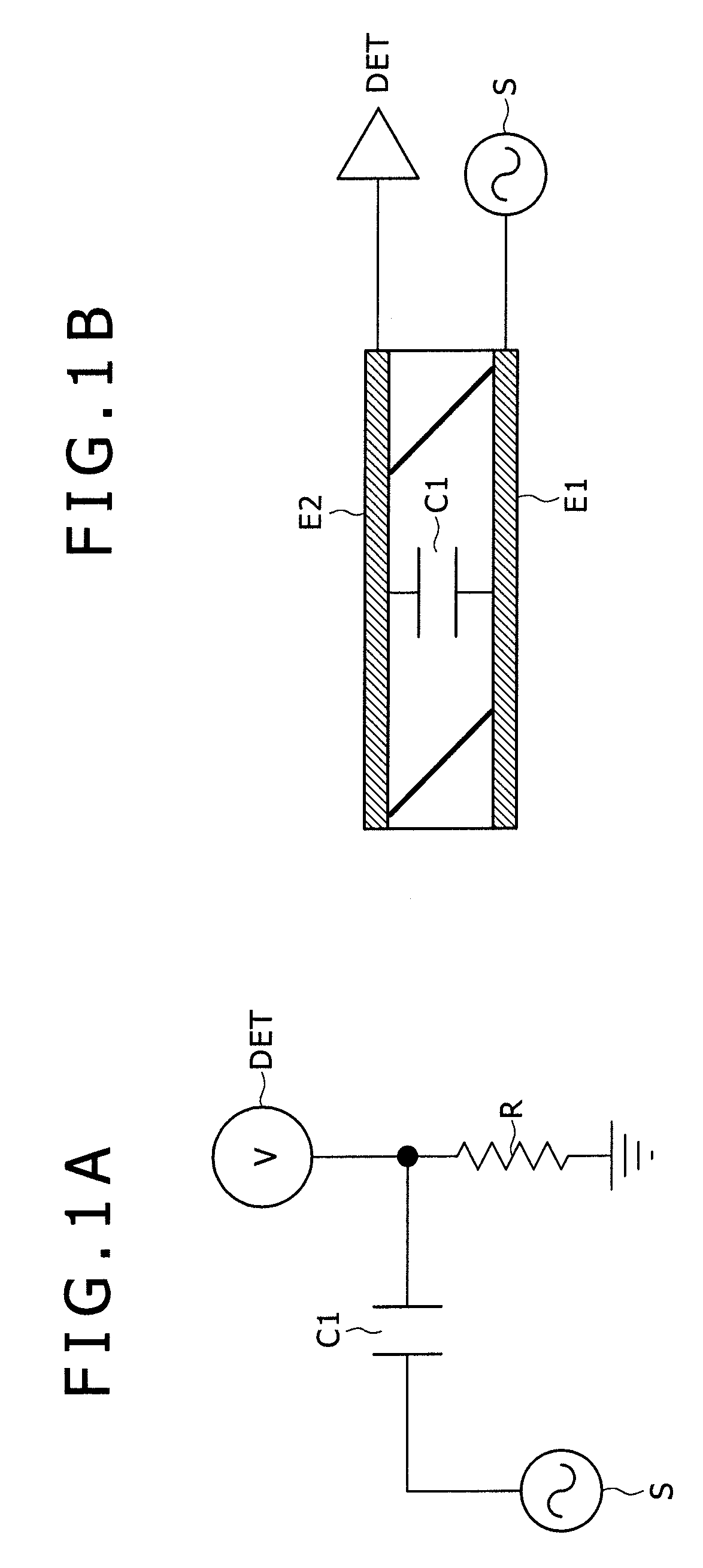
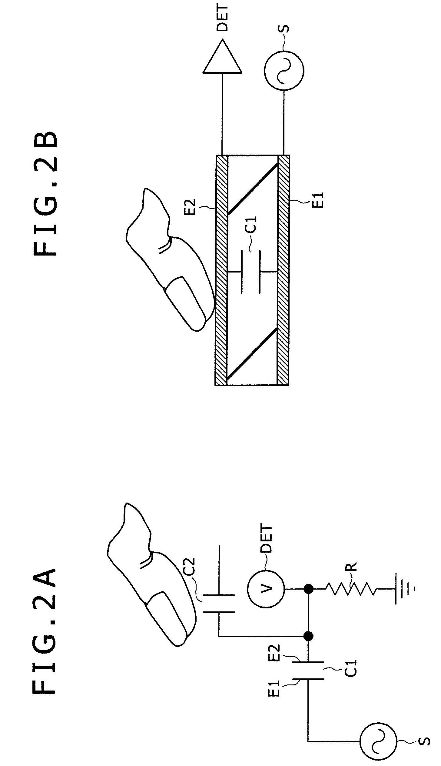
[0068]In the present embodiment, description will be made of an embodiment of a contact detecting device according to the present invention by taking a capacitance type touch panel externally attachable to a display panel as an example.
[0069]FIGS. 4A to 4C are plan views specialized for an arrangement of electrodes of the contact detecting device according to the present embodiment and circuits for driving the electrodes and for detection. FIG. 4D schematically shows a sectional structure when the contact detecting device according to the present embodiment is externally attached to the display surface side of a liquid crystal display device. FIG. 4D shows a section of six pixels in a row direction (pixel display line direction), for example.
[0070]In FIG. 4D, for easy viewing of the sectional structure, counter electrodes, pixel electrodes, and detecting electrodes are hatched, whereas hatching of other parts (substrates, insulating films, functional films and the like) is omitted. ...
second embodiment
[0120]In the present embodiment, in a case of a plurality of regions, for example a case where the number of regions is two, contact driving voltages having different amplitude levels are supplied to a first region Re1 and a second region Re2.
[0121]FIG. 7 shows response waveforms when the number of regions and the number of amplitude levels are two. FIG. 8 and FIG. 9 show response waveforms when the number of regions and the number of amplitude levels are three.
[0122]In the embodiment shown in FIG. 7, a driving voltage supplied to a first set EU11 of driving electrodes in the first region Re1 is different in amplitude from a driving voltage supplied to a second set EU12 of driving electrodes in the second region Re2. FIG. 7 illustrates a case where the amplitude of the latter driving voltage is substantially twice the amplitude of the former driving voltage. The two driving voltages are in phase with each other.
[0123]The second embodiment is the same as the first embodiment except t...
third embodiment
[0132]Two sets EU2 of k detecting lines are provided in the present embodiment.
[0133]FIG. 10 shows response waveforms in a case of opposite-phase driving. FIG. 11 shows response waveforms in a case of in-phase driving.
[0134]The third embodiment is the same as the first and second embodiments in that the third embodiment has a set of detecting lines that intersect a first region Re1 and a second region Re2 in a same manner (which set will hereinafter be referred to as a first set EU21), as shown in FIG. 10 and FIG. 11. The present embodiment is further provided with another set of k detecting lines that intersect only the second region Re2. The k additional detecting lines will hereinafter be referred to as a second set EU22 of detecting lines.
[0135]A detecting circuit 8a including k voltage detectors DETa is connected to one end of the first set EU21 of detecting lines. Similarly, a detecting circuit 8b including k voltage detectors DETb is connected to one end of the second set EU2...
PUM
 Abstract
Description
Claims
Application Information