Touch panel device

a technology of touch panel and input device, which is applied in the field of touch panel devices, can solve the problems of difficult to detect a position, difficult to press a small area or input a character and inability to input a position with high definition by inputting with a finger

Inactive Publication Date: 2010-03-18
MITSUBISHI ELECTRIC CORP
View PDF9 Cites 97 Cited by
  • Summary
  • Abstract
  • Description
  • Claims
  • Application Information

AI Technical Summary

Benefits of technology

[0016]An object of the present invention is to enable, in a capacitive touch panel in which a capacitance detection circuit

Problems solved by technology

On the other hand, an area of the finger per se is larger compared with a pen's tip, and hence it is difficult to press a small area or input a character by inputting with a finger.
Therefore, it is impossible to input a position with high definition by inputting with a finger.
Then, even when the stylus pen touches a touch screen, the capacitance formed by the touch screen and the pen tip electrode is considerably small in proportion to an area

Method used


Image

  • Touch panel device
  • Touch panel device
  • Touch panel device

Examples


Embodiment Construction

[0033]Hereinafter, the present invention will be specifically described with reference to the drawings by way of an embodiment.

[0034](Configuration)

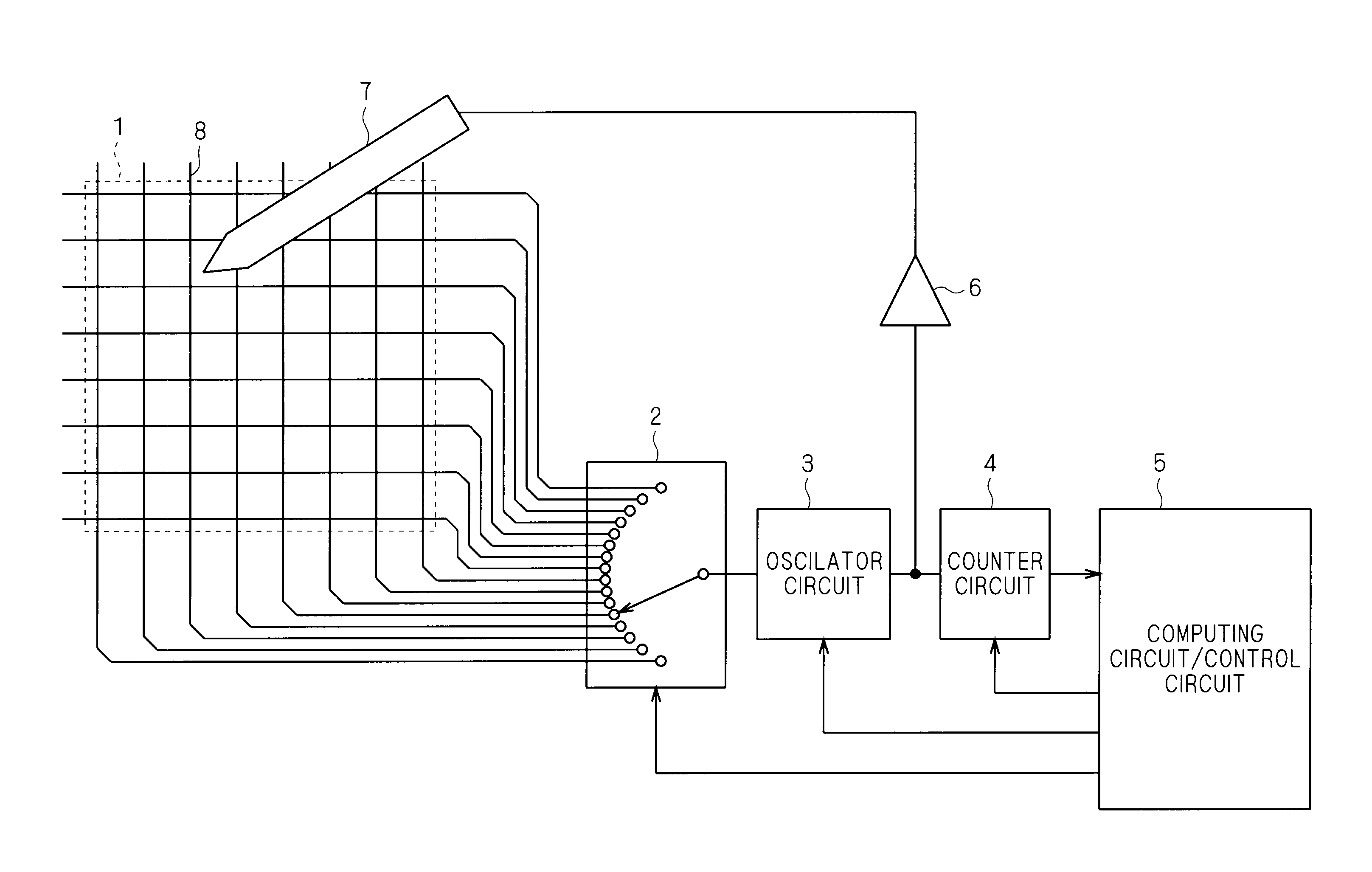
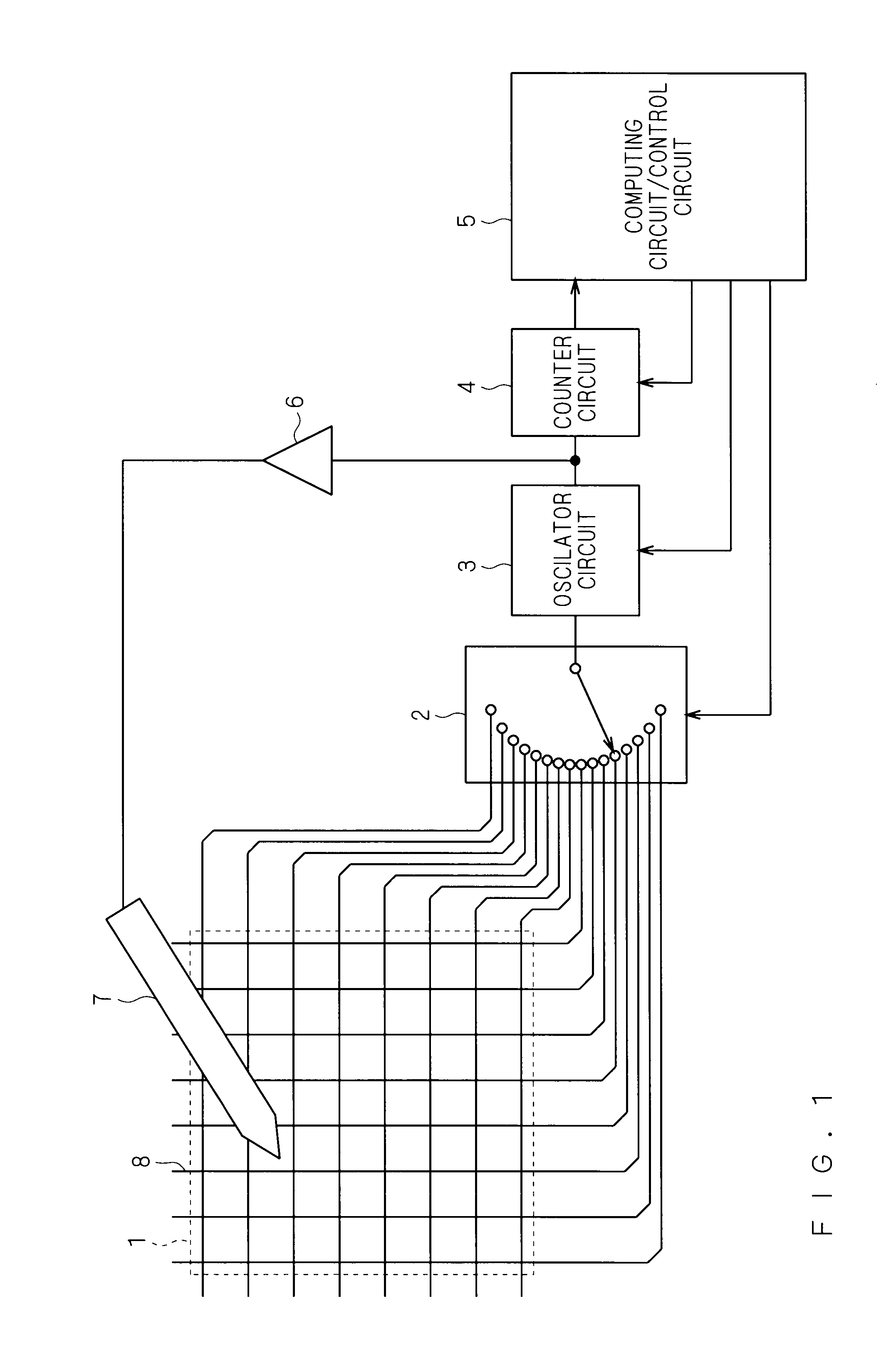
[0035]FIG. 1 is a configuration diagram of a touch panel device thereof according to the present invention, which includes a stylus pen (input pen) 7 including a conductive electrode at a tip portion. The configuration thereof will be described below.

[0036]In a touch screen 1, a plurality of capacitance detecting interconnections 8 which are formed on a substrate in row and column directions are provided, and the capacitance detecting interconnections 8 are individually connected to a plurality of output sections of an interconnection selector circuit 2. An input section of the interconnection selector circuit 2 is connected to an output section of an oscillator circuit (oscillating section) 3, and an input section of the oscillator circuit 3 is connected to an output section of a counter circuit 4. In addition, the output section of the...


PUM


Abstract

A touch panel device according to the present invention includes: a stylus pen including a conductive stylus pen electrode portion at a tip portion thereof; a plurality of capacitance detecting interconnections formed on a substrate in row and column directions; an oscillator circuit which outputs an oscillation signal for performing charging/discharging to each of the plurality of capacitance detecting interconnections, the oscillation signal having a cycle which changes in accordance with an amount of electric charges in the charging/discharging; and a counter circuit and a computing circuit/control circuit which compute, based on a change of the cycle being in accordance with a capacitance formed between the electrode portion of the stylus pen and the capacitance detecting interconnections, positional coordinates of the stylus pen brought in proximity to the capacitance detecting interconnections in a non-contact manner, wherein the stylus pen outputs to the electrode portion of the stylus pen an input pen signal which is in synchronization with the oscillation signal, has a phase different from a phase of the oscillation signal, and has a larger voltage amplitude compared with the oscillation signal.

Description

BACKGROUND OF THE INVENTION[0001]1. Field of the Invention[0002]The present invention relates to a touch panel device including an input pen.[0003]2. Description of the Background Art[0004]In order to detect an input position on a touch panel, there are provided various types of touch panels, such as resistive touch panels, infrared scan touch panels, surface acoustic wave touch panels, acoustic pulse recognition touch panels, touch panels with infrared image sensor and capacitive touch panels. Of those, the capacitive touch panels are classified into a projected capacitive touch screen (hereinafter, referred to as PCT) and a surface capacitive touch screen, in which an input position of a finger is detected by detecting a capacitance change between the finger of an operator and a touch panel detection electrode wire.[0005]In the PCT, it is possible to detect touch even when a front surface side of a touch screen containing a touch sensor is covered with a protective plate such as a...

Claims


Application Information

Patent Timeline
IPC IPC(8): G06F3/041
CPCG06F3/044G06F3/03545G06F3/0441G06F3/0442G06F3/0446
Inventor SATO, IWAOMORI, SEIICHIROMURAI, HIROYUKI
Owner MITSUBISHI ELECTRIC CORP
Why Eureka
Try Eureka