Active matrix display

a technology of active matrix and display, which is applied in the direction of instruments, solid-state devices, semiconductor devices, etc., can solve the problems of increasing parasitic capacity and unable to achieve desired white brightness

Active Publication Date: 2010-04-01
JAPAN DISPLAY CENTRAL CO LTD
View PDF7 Cites 203 Cited by
  • Summary
  • Abstract
  • Description
  • Claims
  • Application Information

AI Technical Summary

Problems solved by technology

A problem with this case is that a desired white brightness cannot be obtained, although the area of the OLED can be increased.
Factors of this problem include increase in parasitic capacity due to overlap between a gate of a drive transistor or an electrode electrically equivalent to this gate and an anode of the OLED over a large area.

Method used


Image

  • Active matrix display
  • Active matrix display
  • Active matrix display

Examples


first embodiment

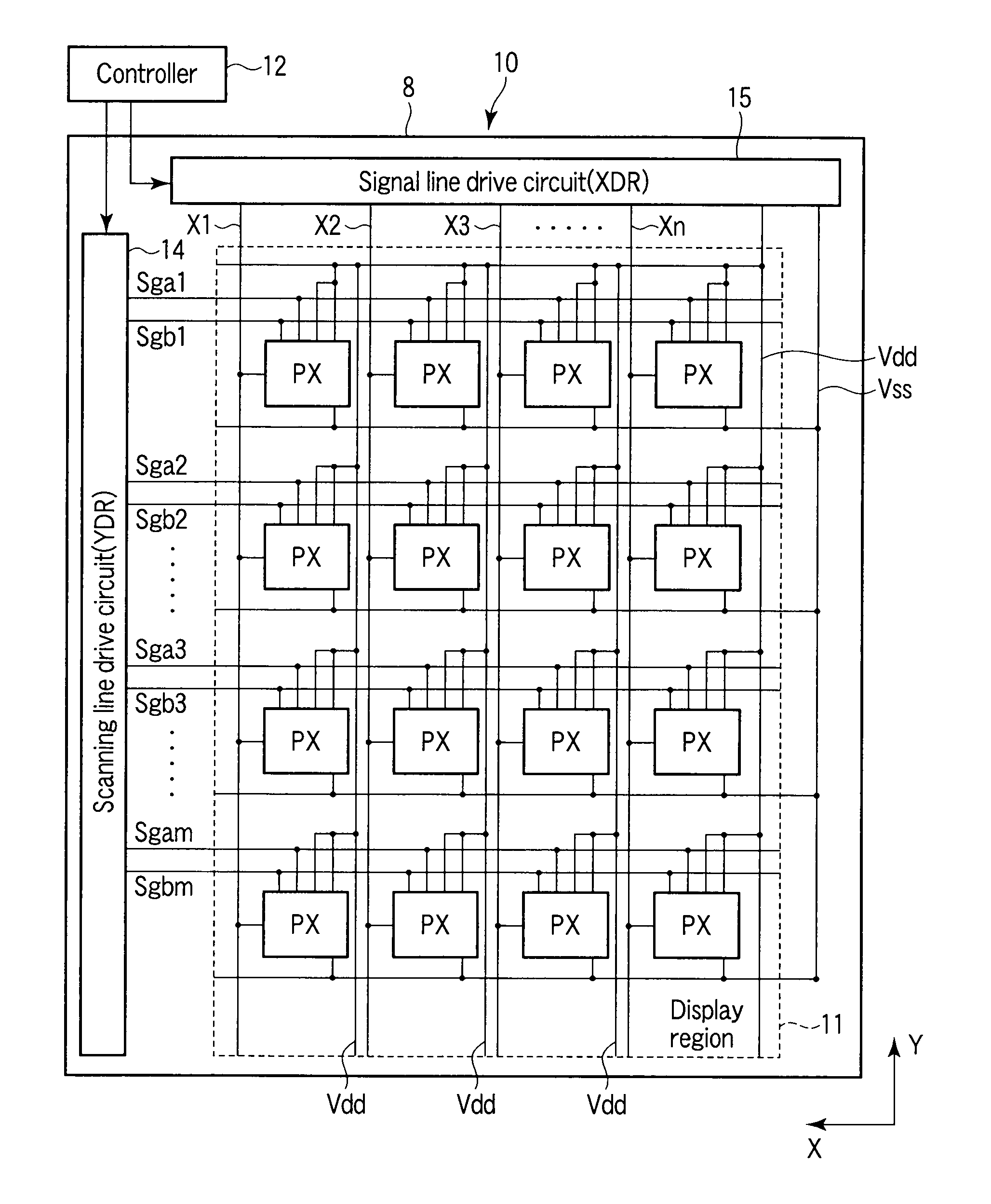
[0026]FIG. 1 is a plan view schematically illustrating an organic EL display according to the present invention. As shown in FIG. 1, a display is a top-emission organic EL display which adopts the active matrix driving scheme. This display includes a display panel 10 and a controller 12 which controls operations of the display panel 10.

[0027]The display panel 10 includes an insulating substrate 8 having optical transparency such as a glass plate, m by n display pixels PX arranged as a matrix on the insulating substrate 8 and forming a display region 11, m first scanning lines (gate wiring for controlling signal writing) Sga (1-m) and m second scanning lines (gate wiring for controlling EL emission) Sgb (1-m) connected to the respective rows of the display pixels and provided independently, and n video signal lines X (1-n) connected to the respective lines of the display pixels PX. The video signal lines X extend in a direction Y (first direction), respectively, and the scanning line...

second embodiment

[0072]Next, an organic EL display will be described.

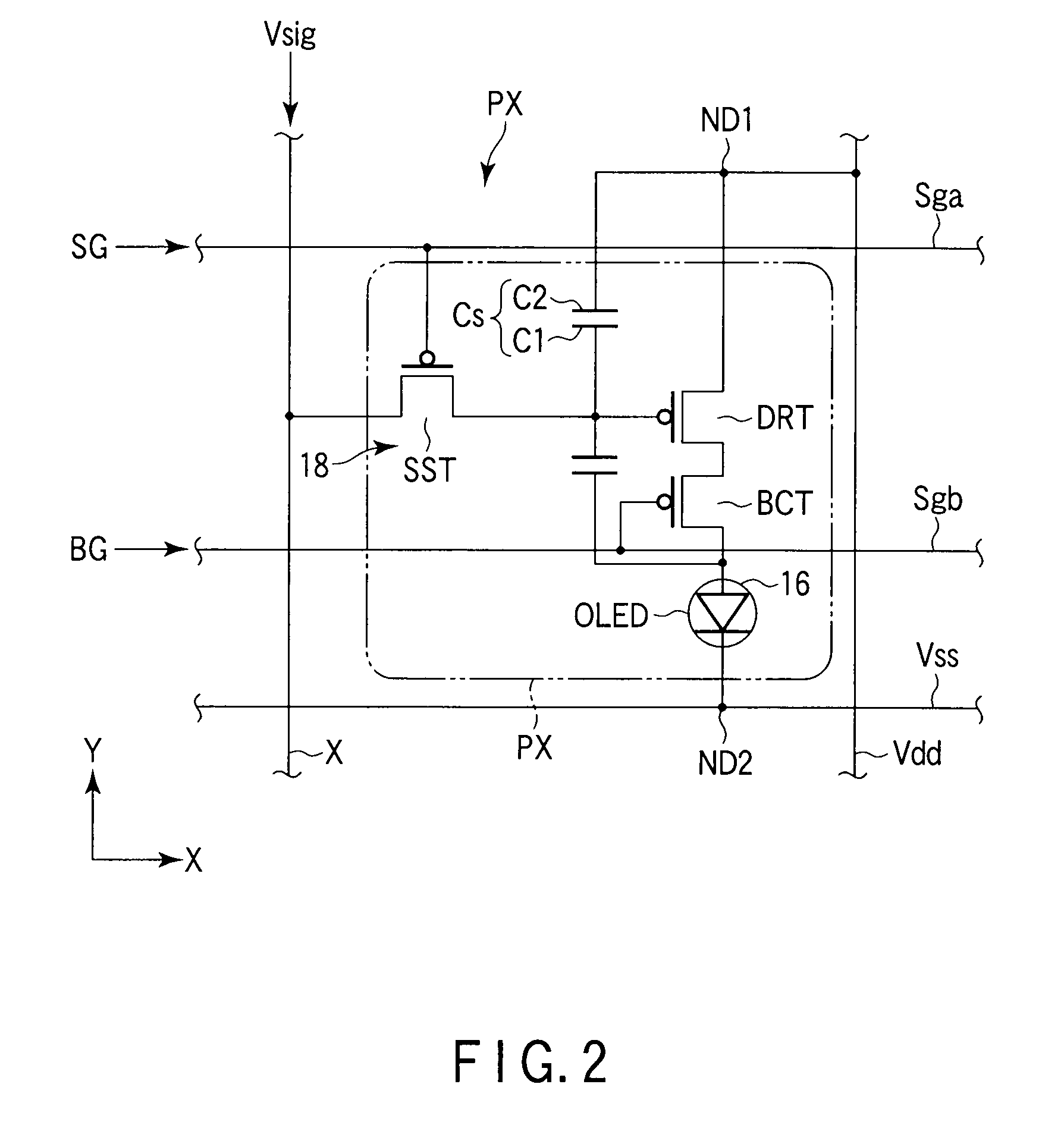
[0073]FIG. 5 is an equivalent circuit diagram of a display pixel of the organic EL display, and FIG. 6 is a plan view schematically illustrating the display pixel.

[0074]The second embodiment is different from the first embodiement in that a shield electrode is provided between an electrode of an organic EL element 16 and an upper electrode of a storage capacitor Cs, and connected to a storage capacity line.

[0075]As shown in FIG. 4, each display pixel PX of the organic EL display includes the organic EL element 16 including a photoactive layer between counter electrodes, and a pixel circuit 18 which supplies a driving current to this element. The pixel circuit 18 is a pixel circuit of a voltage signal scheme of controlling light emission of the organic EL element 16 according to a video signal formed of a voltage signal, and includes a pixel switch SST, a drive transistor DRT, a storage capacitor Cs as a capacitor and an output swi...

third embodiment

[0090]Next, an organic EL display will be described.

[0091]FIG. 7 is an equivalent circuit diagram of the display pixel of the organic EL display, and FIG. 8 is a plan view of schematically illustrating the display pixel. The third embodiment is different from the second embodiment in that the output switch BCT and the second scanning line which controls the output switch to be turned on or off are omitted.

[0092]As shown in FIG. 7, a display pixel PX of the organic EL display includes an organic EL element 16, and a pixel circuit 18 which supplies a driving current to the organic EL element 16. The pixel circuit 18 is a pixel circuit of a voltage signal scheme of controlling light emission of the organic EL element 16, and comprises a pixel switch SST, a drive transistor DRT, a storage capacitor Cs as a capacitor, and a shield electrode 36.

[0093]The pixel switch SST and the drive transistor DRT are formed of P-channel thin-film transistors, for example. The drive transistor DRT is c...


PUM


Abstract

An active matrix display includes a substrate, a video signal line on the substrate, first and second power lines on the substrate, a self-emitting element having two display electrodes facing each other and connected to one of the first and second power lines, a drive transistor connected between the first power line and one of the display electrodes, a storage capacitor having a first electrode connected to a gate electrode of the drive transistor and a second electrode facing the first electrode with interposing an insulating layer, the storage capacitor and the gate electrode of the drive transistor being arranged under the display electrode, and a shield electrode arranged between the display electrode connected to the drive transistor and at least one of the first electrode of the storage capacitor and the gate electrode with interposing an insulating layer, and set at a constant potential.

Description

CROSS-REFERENCE TO RELATED APPLICATIONS[0001]This application is based upon and claims the benefit of priority from prior Japanese Patent Application No. 2008-254526, filed Sep. 30, 2008, the entire contents of which are incorporated herein by reference.BACKGROUND OF THE INVENTION[0002]1. Field of the Invention[0003]This invention relates to an active matrix display including a light-emitting device.[0004]2. Description of the Related Art[0005]Recently, in the field of active matrix displays, attention has been paid to organic electroluminescence (EL) displays using self-luminous elements, on which research and development is conducted actively. For example, an organic EL display disclosed in Jap. Pat. Appln. KOKAI Publication No. 2007-10993 comprises a plurality of pixels arranged in a plurality of lines and rows on a substrate and forming a display screen, and a plurality of video signal lines connected to the respective pixels. Each pixel is formed of an organic EL device, which ...

Claims


Application Information

Patent Timeline
Patent Type & Authority Applications(United States)
IPC IPC(8): G09G5/00
CPCH01L2251/5315H01L27/3272H10K59/126H10K2102/3026
Inventor SHIBUSAWA, MAKOTO
Owner JAPAN DISPLAY CENTRAL CO LTD
Why Eureka
Try Eureka