Radio frequency circuit, radio frequency power amplifier, and semiconductor device

Inactive Publication Date: 2010-04-01
PANASONIC CORP
View PDF13 Cites 11 Cited by
  • Summary
  • Abstract
  • Description
  • Claims
  • Application Information

AI Technical Summary

Benefits of technology

[0011]Therefore, an object of the present invention is to solve the problem that a load impedance cannot be controlled appropriately and that an insertion loss is increased, and to provide a radio frequency circuit, a radio frequency power amplifier, and a semiconductor device which are suitable for multiband operation and / or multimode operation.
[0013]In some cases, it can occur that a load impedance looking from the amplifier circuit toward the output side of the amplifier circuit varies in accordance with a predetermined parameter of the amplified signal. Moreover, in some cases, it can occur that an optimum load impedance varies in accordance with the predetermined parameter of the amplified signal. Considering this, a load impedance looking from the amplifier circuit toward the output side of the amplifier circuit is converted in the transmission line selected by the selection circuit with use of the above-described configuration, thereby enabling the load impedance in accordance with the variations to be optimized. As a result, it becomes possible to cause each of the transmission lines to have an excellent output characteristic over a wide band, and also possible to realize a radio frequency circuit suitable for multiband operation or multimode operation.
[0023]The present invention can solve the conventional problem that a load impedance cannot be controlled appropriately and that an insertion loss is increased, and can provide a radio frequency circuit, a radio frequency power amplifier, and a semiconductor device which are suitable for multiband operation and / or multimode operation.

Problems solved by technology

Therefore, even if the above-described conventional selection circuit is adopted for the output matching circuit of the radio frequency circuit such that multiband operation or multimode operation can be performed in the radio frequency circuit (radio frequency power amplifier), it is impossible to appropriately control a load impedance looking from the amplifier circuit toward an output side of the amplifier circuit.
Accordingly, even if the above-described conventional selection circuit is introduced for the output matching circuit of the radio frequency circuit such that multiband operation or multimode operation can be performed in the radio frequency circuit (radio frequency power amplifier), an insertion loss is increased.
As described above, the above-described conventional selection circuit has a problem that it is impossible to appropriately control a load impedance and that an insertion loss is increased.
Therefore, even if the above-described conventional selection circuit is adopted for the output matching circuit of the radio frequency circuit, it is impossible to cause each of the transmission lines to have an excellent output characteristic over a wide band, and it is difficult to realize a radio frequency circuit suitable for multiband operation or multimode operation.

Method used


Image

  • Radio frequency circuit, radio frequency power amplifier, and semiconductor device
  • Radio frequency circuit, radio frequency power amplifier, and semiconductor device
  • Radio frequency circuit, radio frequency power amplifier, and semiconductor device

Examples


first embodiment

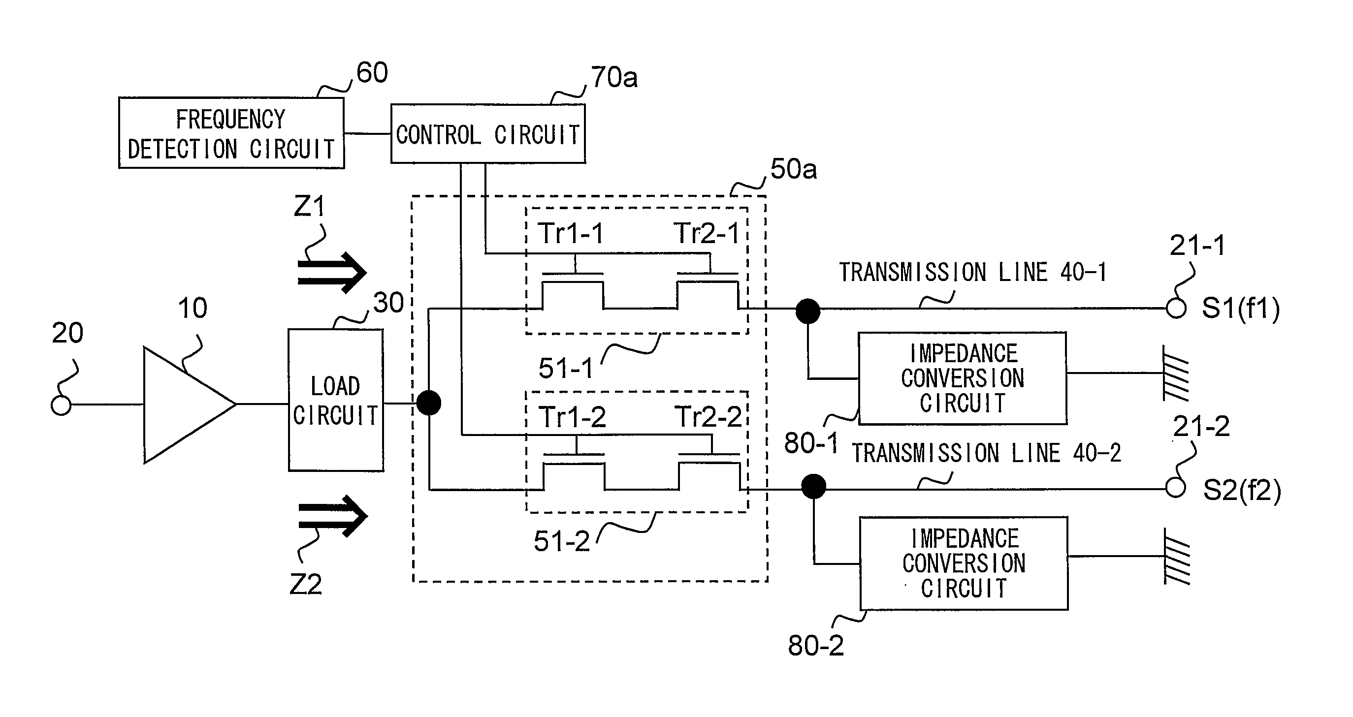
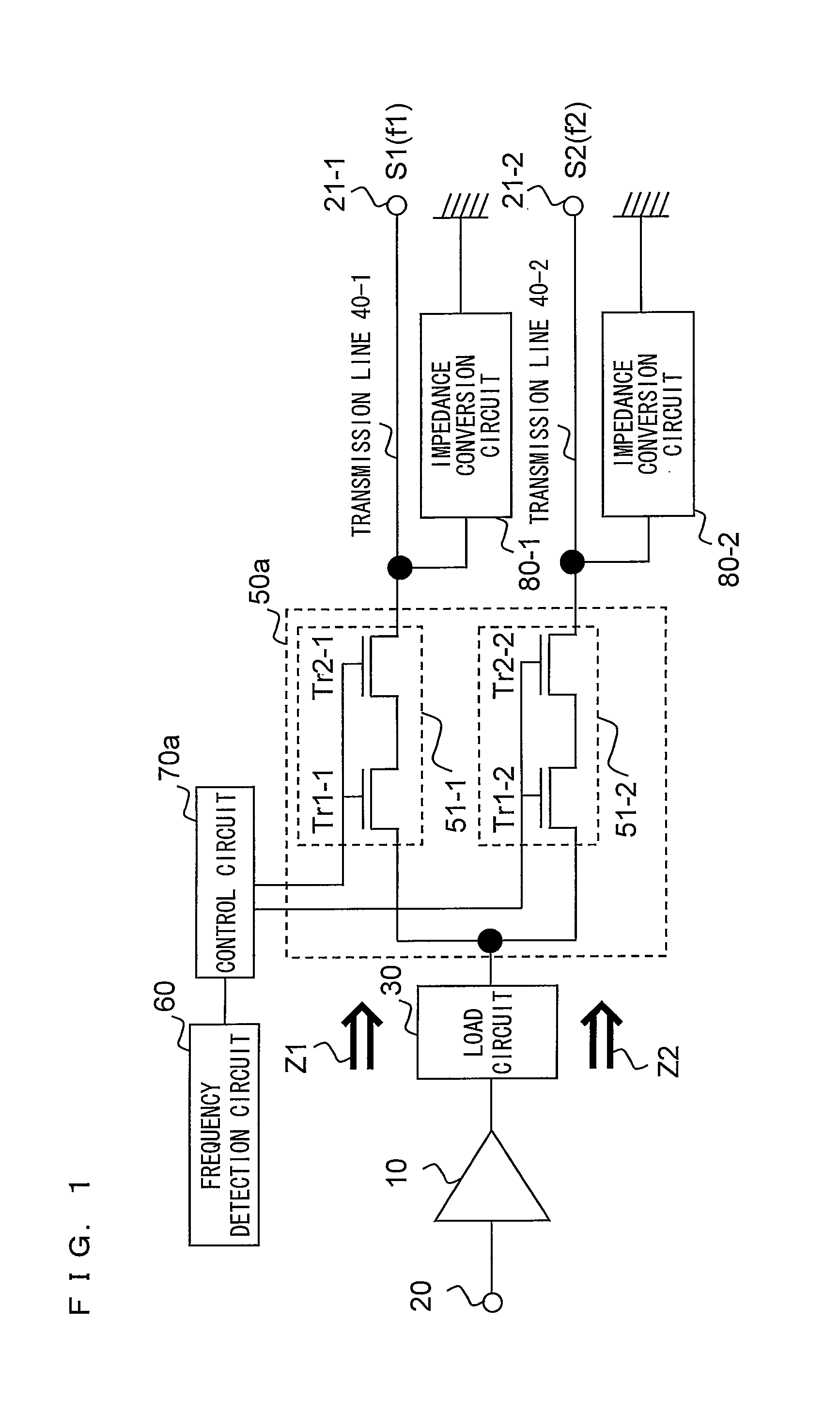
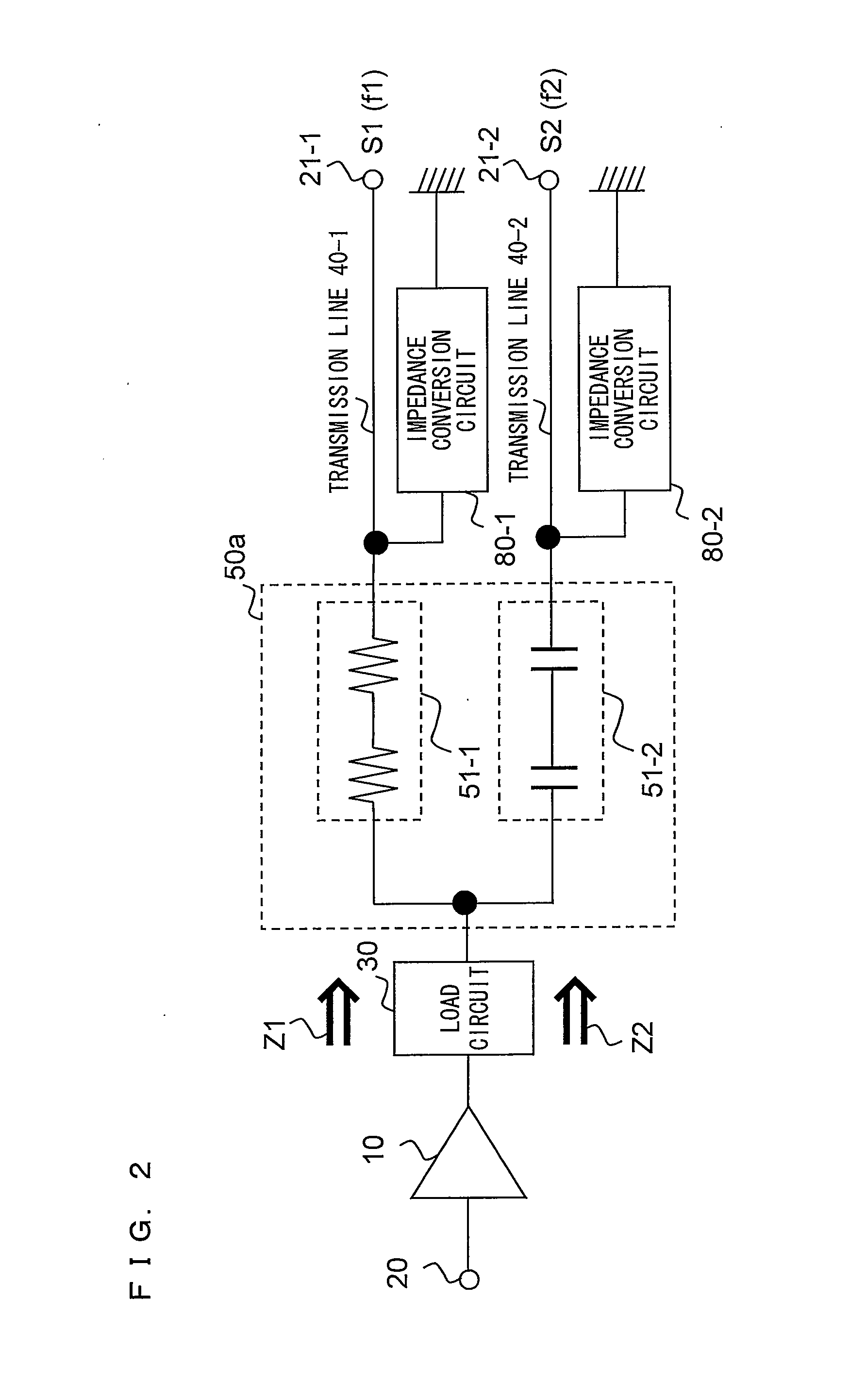
[0048]In a first embodiment, an example of a radio frequency circuit suitable for multiband operation will be described. FIG. 1 is a block diagram showing an example of a configuration of a radio frequency circuit according to the first embodiment of the present invention. In FIG. 1, the radio frequency circuit according to the present embodiment includes an amplifier circuit 10, an input terminal 20, output terminals 21-1 and 21-2, a load circuit 30, transmission lines 40-1 and 40-2, impedance conversion circuits 80-1 and 80-2, a selection circuit 50a, a frequency detection circuit 60, and a control circuit 70a.

[0049]In the example shown in FIG. 1, two kinds of frequencies are used for radio frequency signals. A radio frequency signal S1 has a frequency f1 and a radio frequency signal S2 has a frequency f2. In general, the frequency f1 and the frequency f2 are different from each other, and satisfy, for example, the relationship f12. More specifically, f1 is set to 1710-1785 MHz, ...

second embodiment

[0066]FIG. 5 is a block diagram showing an example of a configuration of a radio frequency circuit according to a second embodiment of the present invention. The radio frequency circuit according to the present embodiment is different from the radio frequency circuit according to the first embodiment shown in FIG. 1, in that the radio frequency circuit according to the present embodiment includes the impedance conversion circuits 80-1 and 80-2 between the load circuit 30 and the selection circuit 50a. Specifically, the radio frequency circuit according to the present embodiment includes the impedance conversion circuits 80-1 and 80-2 between the load circuit 30 and the selection circuit 50a, and further includes switching transistors Tr10-1 and Tr10-2. Hereinafter, differences from the first embodiment will mainly be described. The rest of the configuration of the radio frequency circuit according to the second embodiment, and the operation and effect of the rest of the configuratio...

third embodiment

[0072]FIG. 6 is a block diagram showing an example of a configuration of a radio frequency circuit according to a third embodiment of the present invention. The radio frequency circuit according to the present embodiment is different from the radio frequency circuit shown in FIG. 1 according to the first embodiment, in that the radio frequency circuit according to the present embodiment includes the impedance conversion circuits 80-1 and 80-2 between transistors included in the transistor circuits 51-1 and 51-2, respectively. Specifically, the radio frequency circuit according to the third embodiment includes the impedance conversion circuits 80-1 between the switching transistors Tr1-1 and Tr2-1 on the first path, and the impedance conversion circuits 80-2 between the switching transistors Tr1-2 and Tr2-2 on the second path. Hereinafter, differences from the first embodiment will mainly be described. The rest of the configuration of the radio frequency circuit according to the thir...


PUM


Abstract

A radio frequency circuit according to the present invention, is a radio frequency circuit for amplifying a radio frequency signal, the radio frequency circuit comprising: an amplifier circuit for amplifying the radio frequency signal and outputting an amplified signal obtained by the amplification of the radio frequency signal; a load circuit connected to an output of the amplifier circuit; a plurality of transmission lines; a selection circuit for selecting a transmission line among the plurality of transmission lines in accordance with a predetermined parameter of the amplified signal so as to connect the selected transmission line to an output of the load circuit; and a conversion circuit for converting, into a predetermined load impedance, a load impedance looking from the amplifier circuit toward an output side of the amplifier circuit, the conversion being performed in the transmission line selected by the selection circuit.

Description

BACKGROUND OF THE INVENTION[0001]1. Field of the Invention[0002]The present invention relates to a radio frequency circuit, a radio frequency power amplifier, and a semiconductor device, and more particularly, to a radio frequency circuit, a radio frequency power amplifier, and a semiconductor device which are used for a mobile communication apparatus.[0003]2. Description of the Background Art[0004]A radio frequency power amplifier which is used for a mobile communication device and the like such as a mobile phone, includes a radio frequency circuit including: an amplifier circuit having an amplifying element, such as a transistor, which amplifies a radio frequency signal and outputs the amplified signal; and an output matching circuit for efficiently outputting the amplified signal.[0005]In recent years, while a mobile phone is coming to have multiple functions, multiband operation of transmission signals, and multimode operation in which different modulation signals are used, beco...

Claims


Application Information

Patent Timeline
IPC IPC(8): H04B1/16
CPCH04B1/006H04B1/0483H04B1/0458
Inventor KAIDO, JUNJIINAMORI, MASAHIKOTATEOKA, KAZUKIMATSUDA, SHINGOMAKIHARA, HIROKAZU
Owner PANASONIC CORP
Why Eureka
Try Eureka