Power amplifier circuit

a power amplifier and circuit technology, applied in the direction of duplex signal operation, transmission path division, wireless communication, etc., can solve the problems of limited maximum power supply voltage and transistor breakage, and achieve the effect of improving power-added efficiency

Active Publication Date: 2019-01-08
MURATA MFG CO LTD
View PDF11 Cites 0 Cited by
  • Summary
  • Abstract
  • Description
  • Claims
  • Application Information

AI Technical Summary

Benefits of technology

[0003]Improving of the power-added efficiency in a power amplifier circuit is demanded. To meet this demand, the following technology is known. By boosting the power supply voltage, a load impedance in each amplifier is increased, thereby decreasing the impedance conversion ratio, which is a conversion ratio used for performing impedance matching with a subsequent device in an output matching circuit. As a result, the insertion loss and the return loss in the output matching circuit are reduced. This will be discussed more specifically. When the power supply voltage is about 3.4 V, in order to obtain linear output of about 28.5 dBm, about 4Ω of load impedance is required in an amplifier. In this case, the output matching circuit of the power amplifier circuit converts the load impedance (about 4Ω) of the amplifier into output impedance (about 50Ω, for example) of the power amplifier circuit, and thus, the impedance conversion ratio is about 12.5. If the output matching circuit is constituted by components of a surface mount device (SMD), such as a capacitor and an inductor, and a pattern on a module substrate, it is necessary that the loss in the components forming the output matching circuit be sufficiently smaller than about 4Ω in order to reduce the loss in the output matching circuit. When the power supply voltage is about 10.2 V, which is three times as high as the above-described power supply voltage, in order to obtain linear output of about 28.5 dBm, about 39Ω of load impedance is only required in an amplifier. The impedance conversion ratio in the output matching circuit is about 1.28, which is lower than the above-described impedance conversion ratio. In this case, it is only necessary that the loss in the components forming the output matching circuit be smaller than about 39Ω. In this manner, as a result of increasing the load impedance of an amplifier by boosting the power supply voltage, the loss in the output matching circuit can be reduced, thereby making it possible to improve the power-added efficiency of the power amplifier circuit.
[0004]However, in the power amplifier circuit disclosed in the above-described document “Evolution of Power Amplifier for mobile applications”, the maximum power supply voltage is restricted due to the collector-base withstand voltage of the transistor. In the power amplifier circuit disclosed in the above-described publication, by cascode-connecting two transistors, the divided voltage is applied to each transistor, and thus, the maximum power supply voltage can be increased to be higher than that in the power amplifier circuit in the above-described document. However, the base voltage of the upper-stage transistor is fixed, and when the collector-base voltage of the upper-stage transistor exceeds the withstand voltage, the transistor is broken. The reliability of the power amplifier circuit is thus decreased.
[0005]The present disclosure has been made in view of the above-described background. The present disclosure provides a power amplifier circuit in which the power-added efficiency is improved while the reliability is being maintained.
[0007]According to an embodiment of the present disclosure, it is possible to provide a power amplifier circuit in which the power-added efficiency is improved while the reliability is being maintained.

Problems solved by technology

However, in the power amplifier circuit disclosed in the above-described document “Evolution of Power Amplifier for mobile applications”, the maximum power supply voltage is restricted due to the collector-base withstand voltage of the transistor.
However, the base voltage of the upper-stage transistor is fixed, and when the collector-base voltage of the upper-stage transistor exceeds the withstand voltage, the transistor is broken.

Method used


Image

  • Power amplifier circuit
  • Power amplifier circuit
  • Power amplifier circuit

Examples


first embodiment

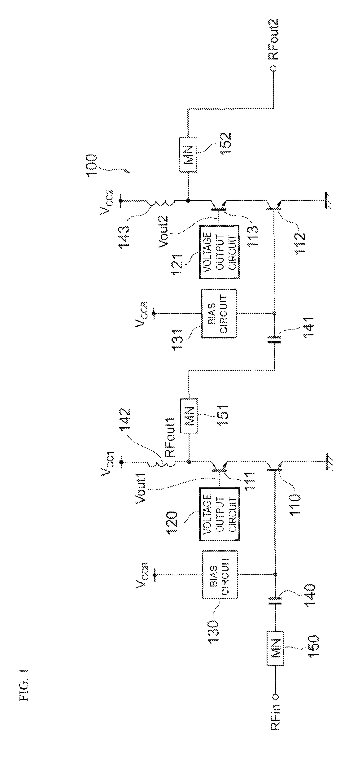
[0030]FIG. 1 illustrates an example of the configuration of a power amplifier circuit 100 according to the disclosure. In a mobile communication device, such as a cellular phone, the power amplifier circuit 100 amplifies an input radio frequency (RF) signal RFin and outputs an amplified signal RFout2. The frequency of the RF signal RFin is about several gigahertz, for example.

[0031]As shown in FIG. 1, the power amplifier circuit 100 includes bipolar transistors 110, 111, 112, and 113, voltage output circuits 120 and 121, bias circuits 130 and 131, capacitors 140 and 141, inductors 142 and 143, and matching circuits 150, 151, and 152.

[0032]The power amplifier circuit 100 includes two-stage amplifiers. The first-stage amplifier (drive stage) includes the bipolar transistors 110 and 111, while the second-stage amplifier (power stage) includes the bipolar transistors 112 and 113. Hereinafter, each pair of the bipolar transistors 110 and 111 and the bipolar transistors 112 and 113 may al...

second embodiment

[0082]FIG. 14 illustrates an example of the configuration of a power amplifier circuit 2000 according to the disclosure. The same elements as those shown in FIG. 1 are designated by like reference numerals, and an explanation thereof will be omitted. The power amplifier circuit 2000 is different from the power amplifier circuit 100 in that, as the upper-stage cascode-connected transistors, field-effect transistors (FETs) 2111 and 2113 are used instead of the bipolar transistors 111 and 113.

[0083]The FET 2111 (second transistor) is cascode-connected to the bipolar transistor 110. The FET 2113 (seventh transistor) is cascode-connected to the bipolar transistor 112. This will be discussed more specifically. A power supply voltage VCC1 is supplied to the drain of the FET 2111 via the inductor 142. The gate of the FET 2111 is connected to the voltage output circuit 120, and the source thereof is connected to the collector of the bipolar transistor 110. A signal amplified by the bipolar t...


PUM


Abstract

A power amplifier circuit includes first and second transistors and a first voltage output circuit. A radio frequency signal is input into a base of the first transistor. The first voltage output circuit outputs a first voltage in accordance with a power supply voltage. The first voltage is supplied to a base or a gate of the second transistor. An emitter or a source of the second transistor is connected to a collector of the first transistor. A first amplified signal generated by amplifying the radio frequency signal is output from a collector or a drain of the second transistor.

Description

[0001]This application claims priority from Japanese Patent Application No. 2016-118183 filed on Jun. 14, 2016. The content of this application is incorporated herein by reference in its entirety.BACKGROUND[0002]The present disclosure relates to a power amplifier circuit. As a power amplifier circuit used in a mobile communication device, such as a cellular phone, “Evolution of Power Amplifier for mobile applications” Satoshi Tanaka, International Meeting for Future of Electron Devices, Kansai (IMFEDK), 2013 IEEE, pp 112-113 discloses a power amplifier circuit using a heterojunction bipolar transistor (HBT). Japanese Unexamined Patent Application Publication No. 2015-115835 discloses a power amplifier circuit including two cascode-connected HBTs.BRIEF SUMMARY[0003]Improving of the power-added efficiency in a power amplifier circuit is demanded. To meet this demand, the following technology is known. By boosting the power supply voltage, a load impedance in each amplifier is increase...

Claims


Application Information

Patent Timeline
Patent Type & Authority Patents(United States)
IPC IPC(8): H03F3/04H03F3/24H03F1/02H03F1/56H03F3/00H03F3/195H03F3/21H04L5/00H04L5/14H03F1/22H04W88/00
CPCH03F3/245H03F1/0272H03F1/0277H03F1/22H03F1/565H03F3/005H03F3/195H03F3/21H04L5/0007H04L5/14H03F1/0205H04W88/00H03F2200/222H03F2200/318H03F2200/387H03F2200/408H03F2200/451H03F2200/555H03F1/0211
Inventor TANAKA, SATOSHIWATANABE, KAZUOTSUTSUI, TAKAYUKIKONDO, MASAOARAYASHIKI, SATOSHIHARIMA, FUMIOHASE, MASATOSHI
Owner MURATA MFG CO LTD
Why Eureka
Try Eureka