Electrical filter device for filtering a common-mode interference between a current source and a load

a technology of electric filter and load, which is applied in the direction of electrical equipment, multiple-port networks, power conversion systems, etc., to achieve the effect of limiting the built-in capacitance of the y capacitor and reducing the loss of insertion

Active Publication Date: 2021-09-02
ROBERT BOSCH GMBH
View PDF0 Cites 0 Cited by
  • Summary
  • Abstract
  • Description
  • Claims
  • Application Information

AI Technical Summary

Benefits of technology

[0026]The coil of the second auxiliary inductance has advantageously been wound onto the first core in the same direction as the coil of the first auxiliary inductance and as the coil of the first main inductance. By virtue of the interconnection of the advantageously one winding of the second auxiliary inductance and the second interference suppression capacitor and the inductive coupling to the first main inductance and advantageously to the first auxiliary inductance, an insertion loss can be improved further for interference frequencies (for example in the range up to a few hundred MHz) than is in any case already possible with only one auxiliary inductance. The resonance behavior of the first auxiliary inductance, the first main inductance and the second auxiliary inductance can advantageously be matched corresponding to desired presets for the filtering effect by virtue of the number of windings of the auxiliary inductances, by virtue of the permeability of the first core, and by virtue of the size of the capacitance of the first and the second interference suppression capacitors. The inductive coupling between the first and second auxiliary inductances and the first main inductance is advantageously complete, in particular when it is large, preferably close to 1.0. The second interference suppression capacitor advantageously has a capacitance which is lower than the capacitance of the main capacitor, as a result of which, advantageously, a loss value with slightly capacitive elements can be achieved than with main capacitors in similarly acting filter circuits which only comprise main stages. This is advantageous since the built-in capacitance of the Y capacitors can be limited.
[0027]The number of windings of the first and the second auxiliary inductances can advantageously be matched for fine tuning of the filtering effect. The first and the second interference suppression capacitors are advantageously both connected in each case to Y capacitors (Cy topology). However, it is also possible for the two interference suppression capacitors to be connected to the respective auxiliary inductance using other topologies or to be supplemented by such other topologies, for example LCL, CLC or other topologies. Furthermore, it is possible to extend the filter device by further auxiliary inductances having further interference suppression capacitors and to inductively couple to the first and / or second main inductance(s).

Problems solved by technology

Owing to increasing miniaturization and increasing complexity of electronics, mutual interfering influences between instrumentation and control and power systems are becoming more present, wherein each electrical device can play the role of an interference sink or interference source for other electrical devices.

Method used


Image

  • Electrical filter device for filtering a common-mode interference between a current source and a load
  • Electrical filter device for filtering a common-mode interference between a current source and a load
  • Electrical filter device for filtering a common-mode interference between a current source and a load

Examples


Embodiment Construction

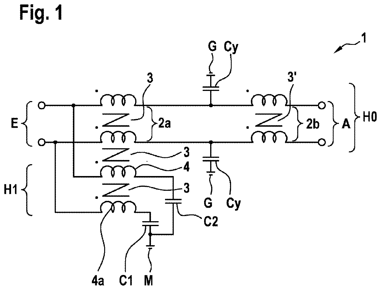
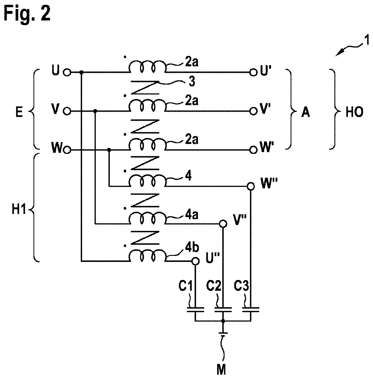
[0042]FIG. 1 shows an electrical circuit diagram for a filter device in accordance with one exemplary embodiment of the present invention.

[0043]The electrical filter device 1 has a signal input E and a signal output A, each advantageously having two contacts, wherein a current source is connectable to the signal input E, and a load, for example an inverter having an electric machine, is connectable to the signal output A. The signal input in this case has a first terminal E1 and advantageously a second terminal E2. The filter device 1 comprises a main stage H0, which comprises a first main inductance 2a at the signal input E, which first main inductance is connected to advantageously the two terminals E1 and E2 of the signal input E, and can advantageously have a second main inductance 2b at the signal output A. The first main inductance 2a can also comprise a plurality of main inductances, which can each be connected to a terminal at the output or input. The first main inductance 2...


PUM


Abstract

The present invention provides an electrical filter device (1) for filtering a common-mode interference between a current source and a load, comprising:—a signal input (E), which comprises at least one first terminal (E1) and can be connected to the current source;—a signal output (A), which can be connected to the load;—a main stage (H0), having a first main inductor (2a), which comprises a coil with a first core (3), the first main inductor (2a) being connected to the first terminal (E1); and—an auxiliary stage (H1), having at least one first anti-interference capacitor (C1) and one first auxiliary inductor (4), the first auxiliary inductor (4) being connected between the first terminal (E1) and the first anti-interference capacitor (C1), the first auxiliary inductor (4) being inductively coupled to the first main inductor (2a).

Description

BACKGROUND OF THE INVENTION[0001]The present invention relates to an electrical filter device for filtering a common-mode interference between a current source and a load.[0002]In the automotive industry, emitted common-mode interference spectra for a pulse-width-modulation inverter (PWMI, for example in the medium-wave range) are reduced (filtered) by common-mode chokes or Y capacitors, passive EMC (electromagnetic compatibility) filters (for example with a different number of stages), by optimized design of motor and cable capacitances, or by special PWM (pulse-width modulation) methods for minimizing common-mode interference. Typical filter topologies such as LC, CLC or LCL generally have insertion losses which, depending on the number of stages, have an edge steepness of up to 40 dB or up to 60 dB per frequency decade. In order to achieve a steeper and / or higher insertion loss, either the nominal component part values of the filter components would need to be increased or a plur...

Claims


Application Information

Patent Timeline
Patent Type & Authority Applications(United States)
IPC IPC(8): H02M1/12H03H7/09
CPCH02M1/123H03H7/09H03H7/1758H03H7/427H02M1/14H02M1/12
Inventor RASEK, GUIDO ALBERTMANUSHYN, ILLIA
Owner ROBERT BOSCH GMBH
Why Eureka
Try Eureka