Method of fabricating device

Inactive Publication Date: 2010-04-15
POWERCHIP SEMICON CORP
View PDF6 Cites 6 Cited by
  • Summary
  • Abstract
  • Description
  • Claims
  • Application Information

AI Technical Summary

Benefits of technology

[0008]Accordingly, the present invention provides a method of fabricating a device, with w

Problems solved by technology

However, the process of reducing the thickness of the tunnel dielectric layer is hard to control, so that manufacturers tend to reduce the thickness of the inter-gate dielectric layer instead.
However, during the nitridation process, an oxynitride layer is formed on the surface of the isolation structures beside the stacked-ga

Method used


Image

  • Method of fabricating device
  • Method of fabricating device
  • Method of fabricating device

Examples


Embodiment Construction

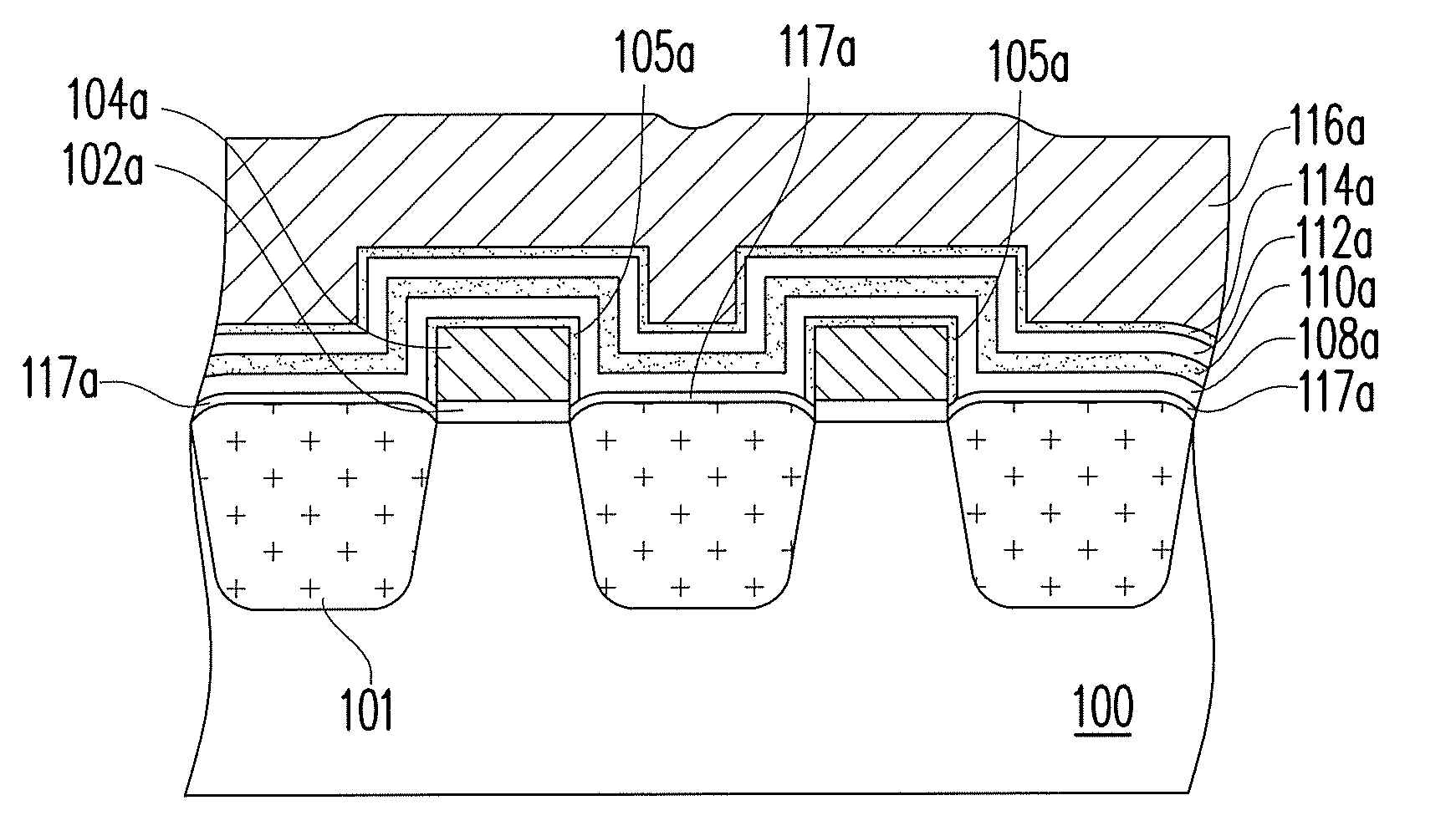
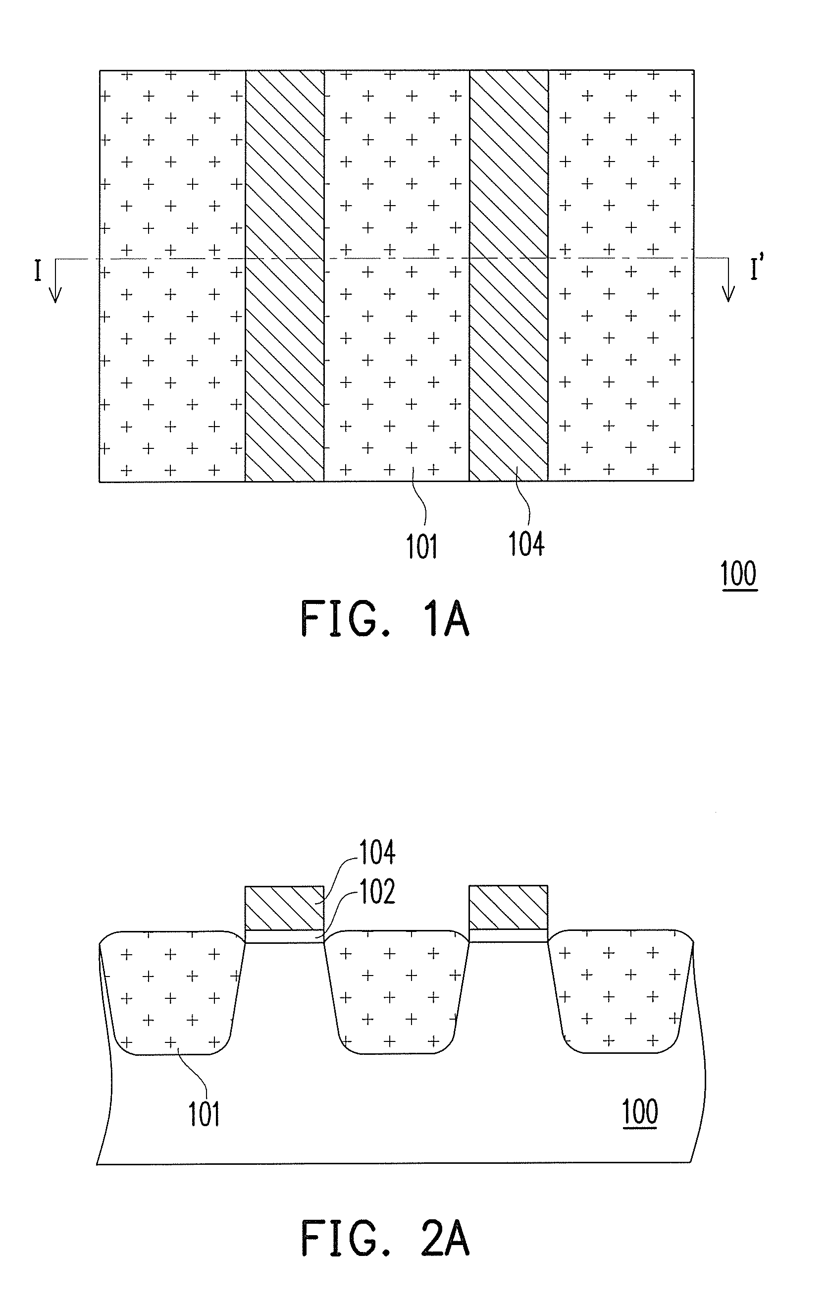
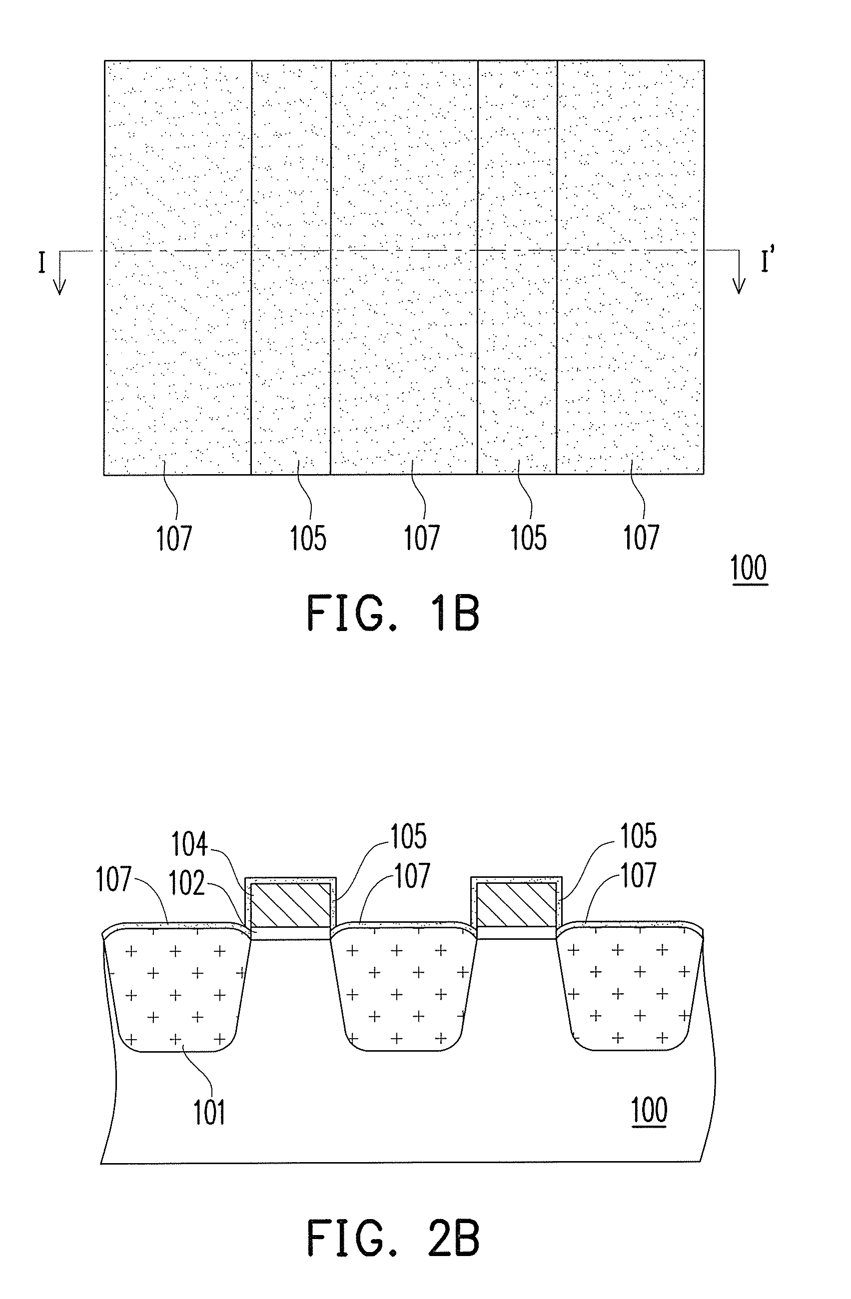
[0025]FIGS. 1A to 1F are schematic top views illustrating a method of fabricating a device according to an embodiment of the present invention. FIGS. 2A to 2F are schematic cross-sectional views taken along the line I-I′ in FIGS. 1A to 1F.

[0026]Referring to FIGS. 1A and 2A, a substrate 100 is provided, and at least two isolation structures 101 have been formed in the substrate 100. In an embodiment, the isolation structures 101 are shallow trench isolation (STI) structures disposed in parallel in the substrate 100. The substrate 100 includes a semiconductor substrate, and the material thereof includes silicon, polysilicon or amorphous silicon, for example. Thereafter, an oxide layer 102 and a conductive layer 104 are sequentially formed on the substrate 100 between the isolation structures 101. The oxide layer 102 includes silicon oxide, for example. The conductive layer 104 includes polysilicon, for example. The method of forming the oxide layer 102 and the conductive layer 104 inc...


PUM


Abstract

A method of fabricating a device is described. A substrate having at least two isolation structures is provided. A first oxide layer and a first conductive layer are sequentially formed on the substrate between the isolation structures. A first nitridation process is performed to form a first nitride layer on the surface of the first conductive layer and a first oxynitride layer on the surface of the isolation structures. A second oxide layer is formed on the first nitride layer and first oxynitride layer. A densification process is performed to oxidize the first oxynitride layer on the surface of the isolation structures. A second nitride layer and a third oxide layer are sequentially formed on the second oxide layer. A second nitridation process is performed to form a third nitride layer on the surface of the third oxide layer. A second conductive layer is formed on the third nitride layer.

Description

BACKGROUND OF THE INVENTION[0001]1. Field of Invention[0002]The present invention relates to a method of fabricating a semiconductor, and more generally to a method of fabricating a device.[0003]2. Description of Related Art[0004]A non-volatile memory provides the property of multiple entries, retrievals and erasures of data, and is able to retain the stored information even when the electrical power is off. As a result, a non-volatile memory is widely used in personal computers and consumer electronic products.[0005]A typical non-volatile memory has a stacked-gate structure, which includes a tunnel dielectric layer, a floating gate, an inter-gate dielectric layer and a control gate sequentially formed on a substrate. As the dimension of a non-volatile memory is getting smaller, how to keep a certain gate coupling ratio (GCR) has become one of the main topics. To achieve the purpose of keeping a certain gate coupling ratio, it is known to thin the tunnel dielectric layer or the inte...

Claims


Application Information

Patent Timeline
IPC IPC(8): H01L21/336H01L21/314
CPCH01L27/11521H10B41/30
Inventor HO, CHING-YUANFUJITA, HIROTAKECHIANG, PO-JUI
Owner POWERCHIP SEMICON CORP
Why Eureka
Try Eureka