Method for producing nonvolatile memory

A non-volatile, manufacturing method technology, applied in semiconductor/solid-state device manufacturing, electrical components, circuits, etc., can solve the problem of not being able to increase the area of ​​the control gate layer and floating gate, increase the gate coupling rate, and increase the number of components Integration and other issues, to prevent short circuit phenomenon, improve component integration, improve the effect of gate coupling rate

CN101064284AInactive Publication Date: 2007-10-31POWERCHIP SEMICON CORP
0 Cites 5 Cited by

Patent Information

Authority / Receiving Office
CN · China
Patent Type
Applications(China)
Current Assignee / Owner
Publication Date
2007-10-31
Estimated Expiration
Not applicable · inactive patent

Smart Images

  • Figure 1
    Figure 1
  • Figure 2
    Figure 2
  • Figure 3
    Figure 3
Patent Text Reader

Abstract

A preparing method of nonvolatile memory is disclosed. Firstly, providing a basis with several separation configurations which extrude the surface of basis, the first mask layer is formed on basis between separation configurations. The second mask layer is formed on the basis. Then, the second mask layer and the first mask layer are patterned to form several openings; these openings expose part of the basis and surface of the separation configurations. Then forming the tubular floating grid which through the dielectric layer and possesses hollows, said tubular floating grid is at the position that adjacent separation configurations and the first mask layer encircle. Then the grip gap dielectric layer is formed on the basis. Then control gate electrode is formed on the basis to fill the opening.
Need to check novelty before this filing date? Find Prior Art

Description

technical field

[0001] The present invention relates to a semiconductor element, and in particular to a method for manufacturing a nonvolatile memory. Background technique

[0002] Non-volatile memory elements have become widely used in personal computers and electronic devices because they can store, read, and erase data multiple times, and the stored data will not disappear after power off. A memory element used.

[0003] A typical non-volatile memory device is generally designed to have a stacked-gate structure, which includes a floating gate (Floating Gate) and a control gate (Control Gate) made of doped polysilicon. The floating gate is located between the control gate and the substrate, and is in a floating state, not connected to any circuit, while the control gate is connected to the word line (Word Line), and also includes the tunnel oxide layer (Tunneling Oxide) and an inter-gate dielectric layer (Inter-Gate Dielectric Layer) are located between the substrate and...

Examples

Embodiment Construction

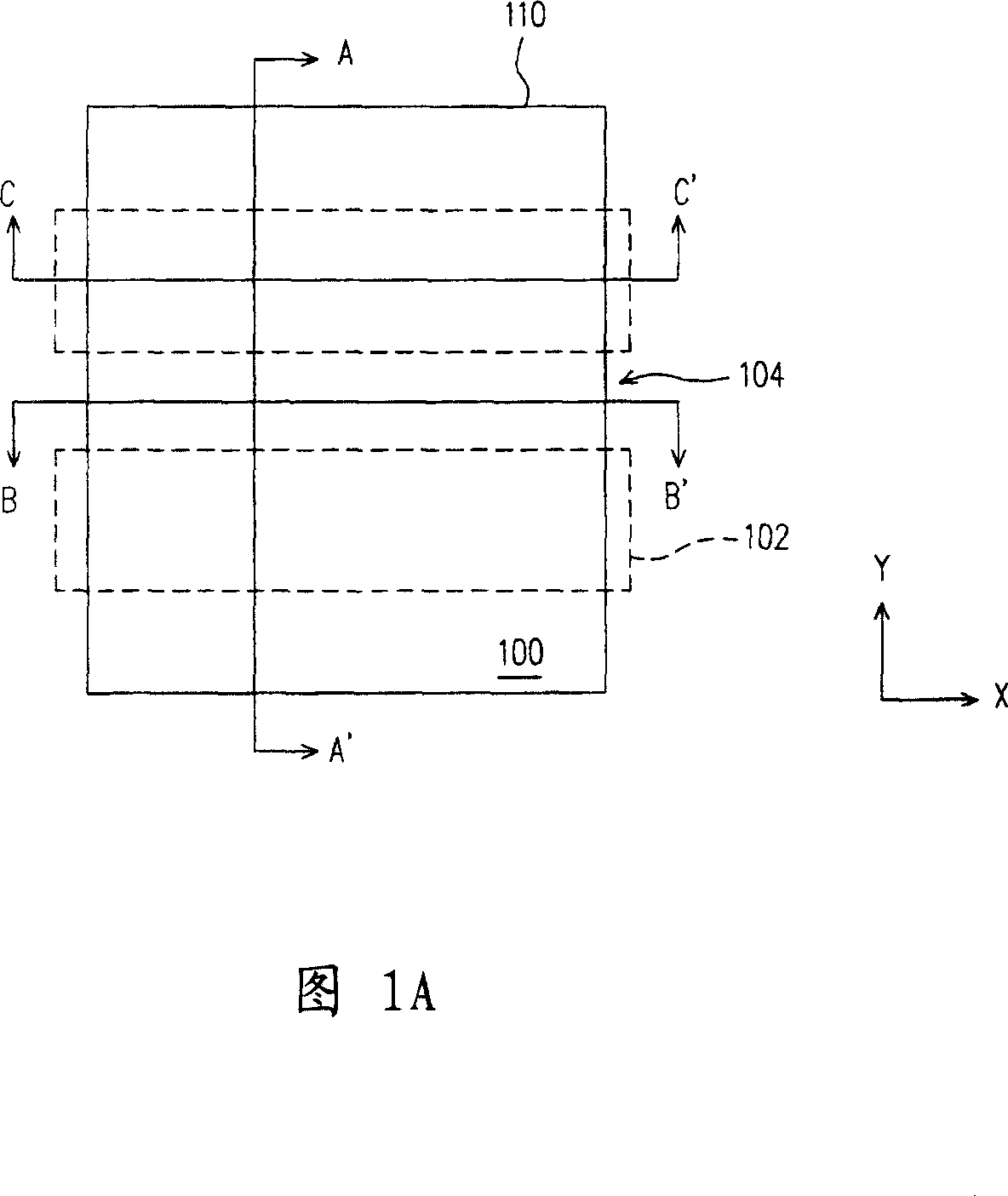
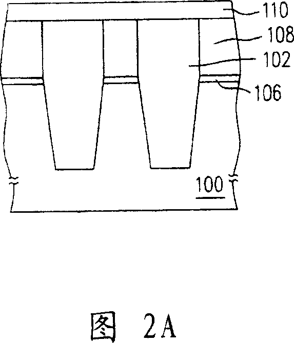
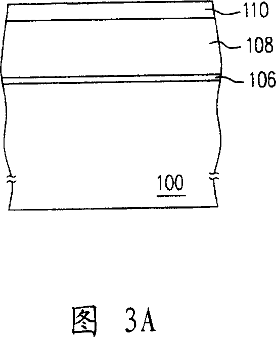
[0052] 1A to 1F are top views illustrating a manufacturing process of a non-volatile memory according to an embodiment of the present invention. 2A to 2F2 are schematic cross-sectional views along line A-A' in FIGS. 1A to 1F respectively. 3A to 3F are schematic cross-sectional views along line B-B' in FIGS. 1A to 1F respectively. FIGS. 4A to 4F are schematic cross-sectional views along line C-C' in FIGS. 1A to 1F . Wherein, A-A' line is a tangent line along the word line; B-B' line is a tangent line along the active region; C-C' is a tangent line along the isolation structure.

[0053] The manufacturing method of the non-volatile memory proposed by the present invention is, for example, suitable for forming NAND gate array flash memory, of course, this manufacturing method can also be used to form other types of non-volatile memory.

[0054] Referring to FIG. 1A , FIG. 2A , FIG. 3A and FIG. 4A , firstly, a substrate 100 is provided. The substrate 100 is, for example, a sili...