
Non-volatile storage and its producing method

A non-volatile, manufacturing method technology, applied in semiconductor/solid-state device manufacturing, electrical solid-state devices, semiconductor devices, etc., can solve problems such as increased manufacturing costs, heat dissipation and noise, and obstacles to increasing memory accumulation, and achieve shortening Manufacturing process, reduction of manufacturing cost, and effect of reduction in the number of photomasks

Inactive Publication Date: 2009-03-11
POWERCHIP SEMICON CORP
View PDF8 Cites 0 Cited by
  • Summary
  • Abstract
  • Description
  • Claims
  • Application Information

AI Technical Summary

Problems solved by technology

In this way, the impact of the short channel effect (Short Channel Effect) will be more significant, which will not only change the enabling voltage (Vt) of the memory, cause problems with the switching of the gate voltage (Vg) control channel, but also cause hot electrons Effect and Punch Through effect, leakage current is generated in the channel, or Electrical Breakdown phenomenon occurs
These situations are very detrimental to the stability and reliability of the memory
[0005] In addition, due to the reduction in the size of the memory cell, the area of ​​the capacitor between the control gate and the floating gate is also reduced, which leads to a decrease in the coupling coefficient of the control gate. When operating the memory cell, it is necessary to apply more high voltage is enough
The increase of operating voltage is likely to cause problems such as heat dissipation and noise, and will also increase power consumption
[0006] Furthermore, although the shallow trench isolation structure has the function of isolating each memory cell column, the fabrication of the shallow trench isolation structure requires photolithography and etching process, which not only increases the manufacturing cost, but also lengthens the entire manufacturing process. Increased speed will also be hindered

Method used


Image

  • Non-volatile storage and its producing method
  • Non-volatile storage and its producing method
  • Non-volatile storage and its producing method

Examples


Embodiment Construction

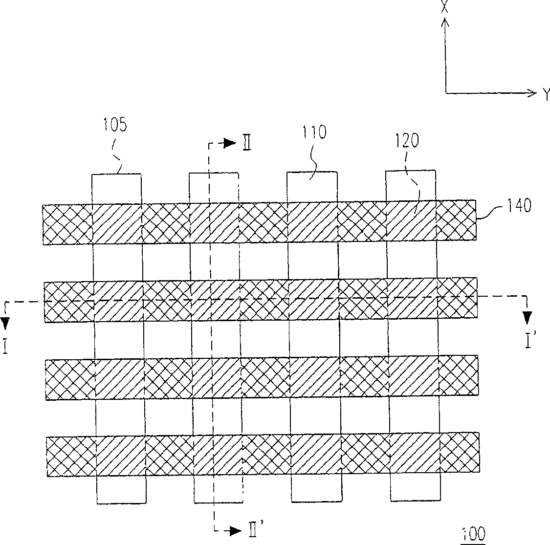
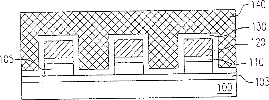
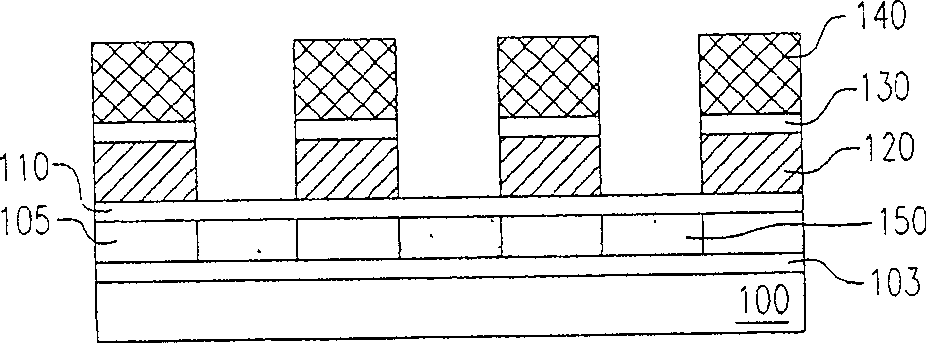
[0040] Figure 1A It is a top view of a non-volatile memory according to an embodiment of the present invention. Figure 1B and Figure 1C to draw separately Figure 1A The cross-sectional view of the structure along the line I-I' and line II-II'.

[0041] Please refer to Figure 1A , Figure 1B and Figure 1C , this non-volatile memory is, for example, a NAND flash memory, which is at least composed of a substrate 100, an insulating layer 103, a plurality of body layers 105, a plurality of tunneling dielectric layers 110, and a plurality of floating gates electrode 120 , a plurality of inter-gate dielectric layers 130 , a plurality of control gates 140 and a plurality of doped regions 150 .

[0042] For example, an insulating layer 103 is disposed on the surface of the substrate 100 . The main body layer 105 is disposed on the base 100 , and the main body layer 105 is arranged in strips in parallel and extends toward the X direction. The control gates 140 are, for exampl...


PUM


Abstract

Non-volatile memory is composed of substrate, multiple main body layers, multiple control grids, multiple floating grids, and multiple doping areas. An insulating layer is on surface of the substrate. Being setup on the substrate, the main body layers in paralleled strips are arranged and extended along the first direction. Being setup on the substrate, the control grids in paralleled strips are arranged and extended along the second direction. The second direction and the first direction are staggered. Moreover, the control grids are filled to gaps of the main body layers along the second direction. The floating grids are setup between control grids and the main body layers. The doping areas are setup in main body layers between control grids.

Description

technical field [0001] The invention relates to a semiconductor element and its manufacturing method, in particular to a non-volatile memory and its manufacturing method. Background technique [0002] The flash memory (Flash) in the non-volatile memory has become one of the mainstream research in the industry due to its fast and time-saving operation mode and cost advantages. A typical flash memory device is mainly composed of a floating gate (Floating Gate) and a control gate (Control Gate). Separated by a dielectric layer, and separated by a tunnel oxide layer (Tunnel Oxide) between the floating gate and the substrate. [0003] Currently, flash memory arrays commonly used in the industry include a NOR gate (NOR) array structure and a NAND gate (NAND) array structure. In the flash memory structure of a NAND array, each memory cell is connected in series, and each column of memory cells is usually isolated by a shallow trench isolation (STI) structure. Its integration and...

Claims


Application Information

Patent Timeline
Patent Type & Authority Patents(China)
IPC IPC(8): H01L27/105H01L21/8239H10B99/00
Inventor 赖亮全
Owner POWERCHIP SEMICON CORP
Learn More