Lead frame unit, package structure and light emitting diode device having the same

a technology of light emitting diodes and lead frame units, which is applied in the direction of semiconductor devices, semiconductor/solid-state device details, electrical apparatus, etc., can solve the problems of troublesome removal of conductive supports, troublesome assembly of conductive supports, etc., and achieve the effect of reducing the total preventing the removal of lead frame units from the insulating housing, and reducing the height of the led devi

Active Publication Date: 2010-04-29
LITE ON TECH CORP +1
View PDF5 Cites 41 Cited by
  • Summary
  • Abstract
  • Description
  • Claims
  • Application Information

AI Technical Summary

Benefits of technology

[0006]Therefore, the object of the present invention is to provide an LED device with an improved lead frame unit, which is attached firmly to an insulating housing in such a manner that the total height of the LED device is decreased and removal of the lead frame unit from the insulating housing is prevented.
[0007]According to an aspect of the present invention, a lead frame unit is adapted to form the LED device. The lead frame unit comprises two conductive bodies. Each of the conductive bodies has a first conductive terminal and a second conductive terminal spaced-apart from each other along an axial direc

Problems solved by technology

The assembly of conductive supports and an insulating housing of a conventional light emitting diode (LED) has a problem.
That is, the process of bending each o

Method used


Image

  • Lead frame unit, package structure and light emitting diode device having the same
  • Lead frame unit, package structure and light emitting diode device having the same
  • Lead frame unit, package structure and light emitting diode device having the same

Examples


Embodiment Construction

[0016]Before the present invention is described in greater detail, it should be noted that like elements are denoted by the same reference numerals throughout the disclosure.

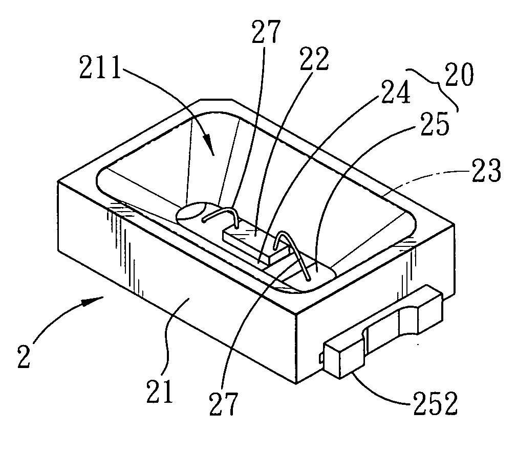
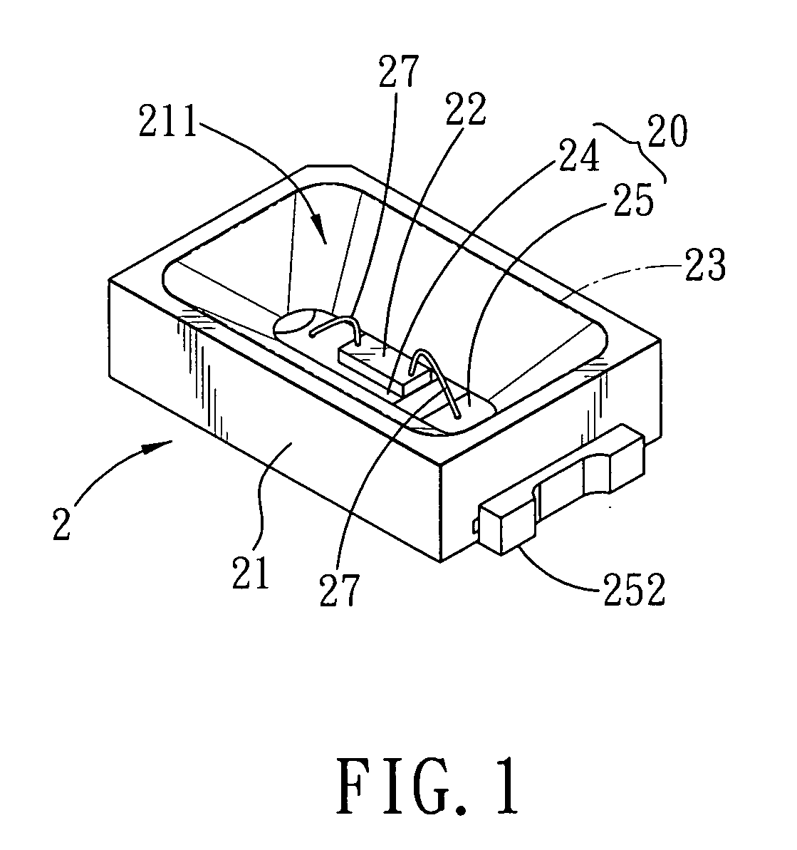
[0017]As shown in FIG. 1, a preferred embodiment of a light emitting diode (LED) device 2 according to the present invention comprises a lead frame unit 20, an insulating housing 21 formed on the lead frame unit 20, an LED die 22 disposed on the lead frame unit 20, and a light transmissive encapsulating material 23 integrated with the insulating housing 21 for covering the LED die 22.

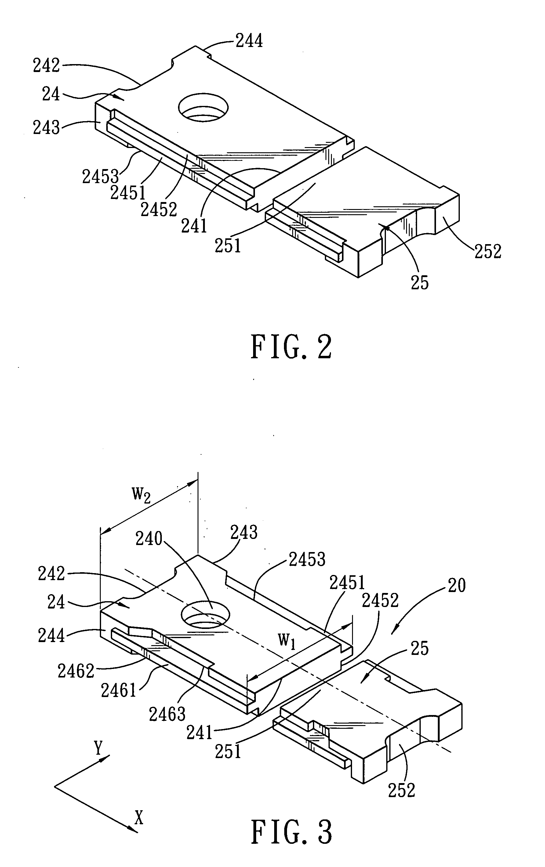
[0018]Further referring to FIGS. 2 and 3, the lead frame unit 20 includes two spaced-apart conductive bodies 24, 25. The conductive body 24 has opposite first and second conductive terminals 241, 242 spaced-apart from each other along an axial direction (X), i.e., a left-to-right direction in the drawings. The conductive body 25 has opposite first and second conductive terminals 251, 252 spaced-apart from each other along the axial ...


PUM


Abstract

A package structure is adapted for mounting at least one light emitting diode (LED) die. The package structure includes an insulating housing, and a lead frame unit including two spaced-apart conductive bodies. Each of the conductive bodies has opposite first and second conductive terminals spaced-apart from each other along an axial direction. The first conductive terminals extend into the insulating housing. The second conductive terminals are exposed outwardly of the insulating housing. Each of the conductive bodies further has two side edges spaced-apart from each other along a transverse direction perpendicular to the axial direction, and a concave-convex structure disposed at the side edges and surrounded by the insulating housing.

Description

CROSS-REFERENCE TO RELATED APPLICATION[0001]This application claims priority of Chinese Patent Application No. 200810218661.6, filed on Oct. 23, 2008.BACKGROUND OF THE INVENTION[0002]1. Field of the Invention[0003]The invention relates to a lead frame unit, more particularly to a lead frame unit adapted for mounting a light emitting diode die, and a package structure having the lead frame unit structure.[0004]2. Description of the Related Art[0005]The assembly of conductive supports and an insulating housing of a conventional light emitting diode (LED) has a problem. That is, the process of bending each of the conductive supports to form a hook end against a bottom part of the insulating housing so as preventing removal of the conductive supports is troublesome. Furthermore, due to such shape of the conductive supports, the total height of the conventional LED device is increased significantly.SUMMARY OF THE INVENTION[0006]Therefore, the object of the present invention is to provide...

Claims


Application Information

Patent Timeline
IPC IPC(8): H01L33/00H01L23/48H01L23/495
CPCH01L24/48H01L33/486H01L2224/48091H01L2224/48247H01L2224/73265H01L2224/32245H01L2924/00014H01L2924/00H01L2224/451H01L2924/12041H01L2224/45099
Inventor LIN, CHEN-HSIU
Owner LITE ON TECH CORP
Why Eureka
Try Eureka