Method for manufacturing silicon single crystal wafer
Active Publication Date: 2010-04-29
SHIN-ETSU HANDOTAI CO LTD
View PDF11 Cites 21 Cited by
Summary
Abstract
Description
Claims
Application Information
AI Technical Summary
This helps you quickly interpret patents by identifying the three key elements:
Problems solved by technology
Method used
Benefits of technology
Benefits of technology
[0041]As explained above, according to the present invention even in the silicon single crystal wafer in which the Ni region and the Nv region are mixedly present, a silicon single crystal wafer that can produce the sufficient BMD in the bulk region and can have a high gettering capability with excellent TDDB characteristics in the wafer entire plane can be manufactured. Furthermore, manufacture can be ca
Problems solved by technology
It has been revealed that a fine defect (which will be also referred to as a Grown-in defect hereinafter) that is formed at crystal growth and adversely affects device performance is present besides the OSF.
This BMD becomes a problem since it adversely affects device characteristics, e.g., a junction leakage when it is generated in a device active region in a wafer but, on the other hand, this BMD i
Method used
Image
Click on the blue label to locate the original text in one second.
Reading with bidirectional positioning of images and text.
Examples
Example
EXAMPLE 1, COMPARATIVE EXAMPLE 1
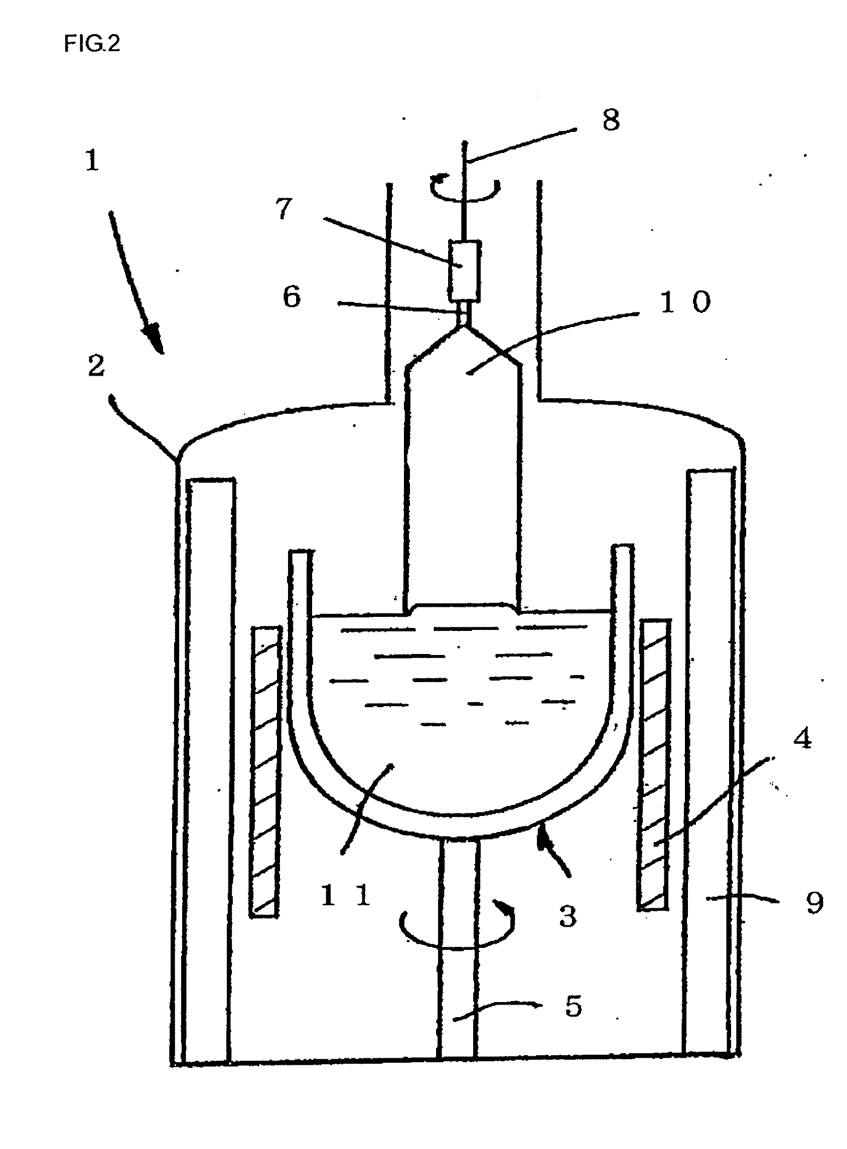
[0083]A p-type silicon single crystal ingot which has a resistivity of 9.2 Ωcm, an initial oxygen concentration of 11.0 ppma (JEIDA), an N region in the entire plane (an Ni region at a central portion, an Nv region at an outer peripheral portion), and a diameter of 300 mm and in which 102 OSFs are detected per cm2 in the outer peripheral portion by a high-sensitivity OSF inspection was grown by using the single-crystal pulling apparatus 1 depicted in FIG. 2, and wafers sliced out from this silicon single crystal ingot and subjected to a chemical etching process were prepared (CW wafers) for Example 1 and Comparative Example 1, respectively.
[0084]As Example 1 corresponding to the manufacturing method according to the present invention, such a rapid thermal annealing apparatus 12 as shown in FIG. 3 was used to increase a temperature of the CW wafer in a dry oxygen atmosphere at a temperature-up speed of 50° C. / s, perform a rapid oxidation heat treatme...
Example
[0088]Further, as Comparative Example 1 corresponding to a conventional manufacturing method, RTA processing on a second stage, thermal simulation simulating a device manufacturing process, and measurement of oxide dielectric breakdown voltage characteristics were performed in the same way as Example 1 except that RTO processing on a first stage and subsequent HF cleaning was not carried out.
[0089]FIG. 4 shows TDDB evaluation results of Example 1 and Comparative Example 1. An abscissa in the graph represents a maximum temperature in the RTO processing on the first stage, and an ordinate of the same represents a percentage of cells in a wafer that are 5C / cm2 or above when a constant current TDDB was evaluated (i.e., a percentage of cells that were not broken even though charged to 5C / cm2) as a yield.
[0090]In the CW wafer utilized this time, TDDB characteristics were lowered in a region of a wafer outer peripheral portion where an OSF was detected in a preliminary high-sensitivity OSF...
Example
EXAMPLE 2, COMPARATIVE EXAMPLE 2
[0092]A p-type silicon single crystal ingot which has a resistivity of 10.2 Ωcm, an initial oxygen concentration of 10.9 ppma (JEIDA), an N region in the entire plane (an Ni region at a central portion, an Nv region at an outer peripheral portion), and a diameter of 300 mm and in which 76 OSFs are detected per cm2 in the outer peripheral portion by a high-sensitivity OSF inspection was grown, and wafers sliced out from this silicon single crystal ingot and subjected to a chemical etching process were prepared (CW wafers) for Example 2 and Comparative Example 2, respectively.
PUM
Abstract
The present invention provides a method for manufacturing a silicon single crystal wafer, in which a silicon single crystal wafer that is fabricated based on a Czochralski method and has an entire plane in a radial direction formed of an N region is subjected to a rapid thermal annealing in an oxidizing atmosphere, an oxide film formed in the rapid thermal annealing in the oxidizing atmosphere is removed, and then a rapid thermal annealing is carried out in a nitriding atmosphere, an Ar atmosphere, or a mixed atmosphere of these atmospheres. As a result, there can be provided the manufacturing method that can inexpensively manufacture a silicon single crystal wafer both in which a DZ layer is formed in a wafer surface layer to provide excellent device characteristics and in which an oxide precipitate functioning as a gettering site can be sufficiently formed in a bulk region.
Description
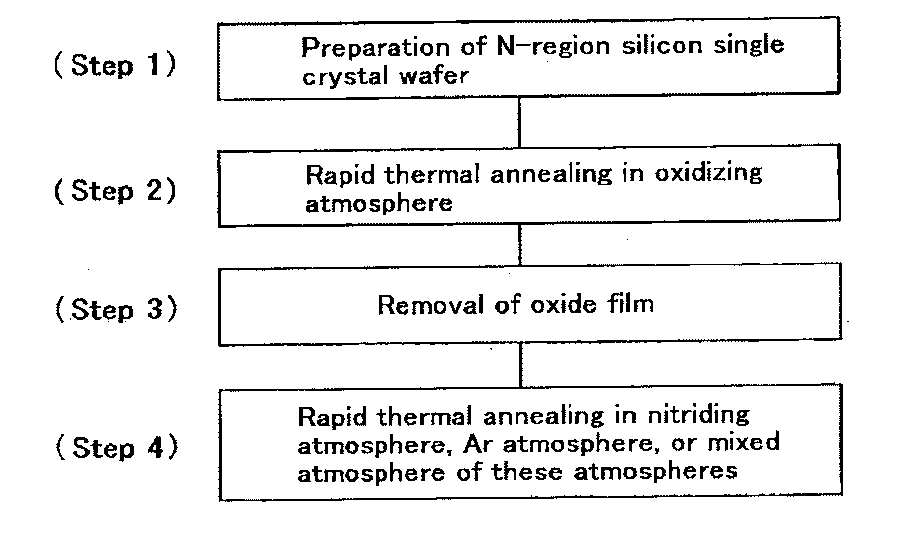
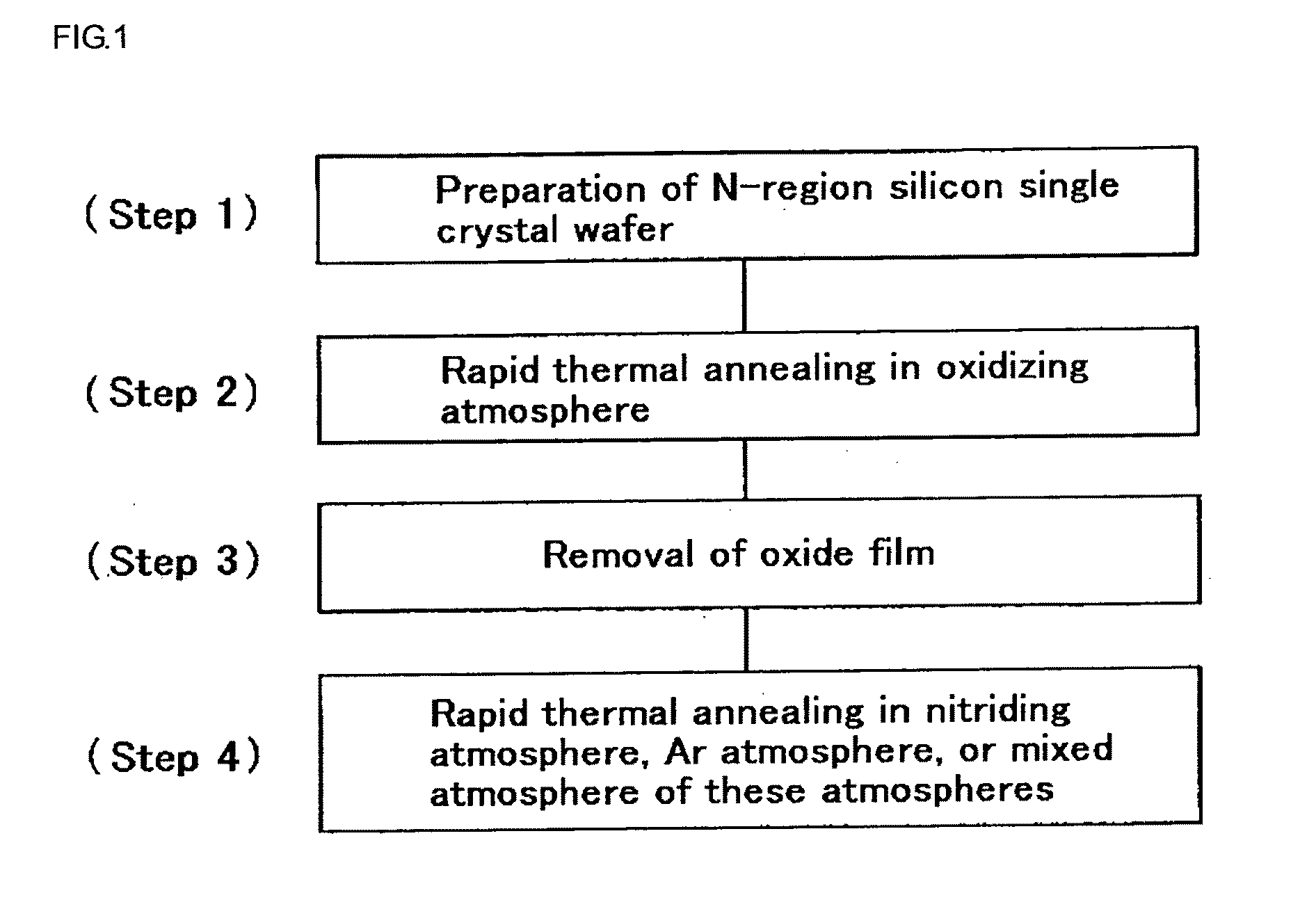
TECHNICAL FIELD[0001]The present invention relates to a method for manufacturing a silicon single crystal wafer that has a DZ layer in which no crystal defect occurs formed at a fixed depth from a wafer surface to a device active region and can form an oxide precipitate that becomes a gettering site in the wafer.BACKGROUND ART[0002]A silicon single crystal wafer serving as a material for a semiconductor device can be generally fabricated by growing a silicon single crystal based on a Czochralski method (which will be also referred to as a CZ method hereinafter) and performing a process, e.g., slicing or polishing with respect to an obtained silicon single crystal.[0003]In the silicon single crystal grown based on the CZ method in this manner, an oxidation induced stacking fault called an OSF that occurs in a ring-like shape may be produced when subjected to thermal oxidation processing (e.g., 1100° C. for two hours). It has been revealed that a fine defect (which will be also referr...
Claims
Application Information
Patent Timeline
Application Date:The date an application was filed.
Publication Date:The date a patent or application was officially published.
First Publication Date:The earliest publication date of a patent with the same application number.
Issue Date:Publication date of the patent grant document.
PCT Entry Date:The Entry date of PCT National Phase.
Estimated Expiry Date:The statutory expiry date of a patent right according to the Patent Law, and it is the longest term of protection that the patent right can achieve without the termination of the patent right due to other reasons(Term extension factor has been taken into account ).
Invalid Date:Actual expiry date is based on effective date or publication date of legal transaction data of invalid patent.

