Liquid crystal display device and manufacturing method therefor

a technology of liquid crystal display and manufacturing method, which is applied in the direction of identification means, instruments, optics, etc., can solve the problems of large influence on glass substrate, and unfavorable uniformity in etching rate, so as to reduce manufacturing process and avoid contact defects , the effect of large manufacturing margin

Inactive Publication Date: 2005-07-21
AU OPTRONICS CORP
View PDF4 Cites 31 Cited by
  • Summary
  • Abstract
  • Description
  • Claims
  • Application Information

AI Technical Summary

Benefits of technology

[0034] The present invention takes into account the present state of the art, not only avoiding the defects in forming the contacts common to the conventional five-mask process and the four-mask process, but also decreasing the manufacturing processes used in half-tone exposure technology having a large manufacturing margin. The need to achieve lower-priced liquid crystal panels and earnestly pursue a further decrease in the number of manufacturing processes in response to increased demand is clear. The value of the present invention is thus further enhanced by its contribution of technology to simplify other major manufacturing processes and provide lower costs.

Problems solved by technology

Still, with the former measure, if the surface uniformity of these film thickness is unfavorable, this approach may not necessarily act effectively either, and this applies identically to cases where the surface uniformity in the etch rate is also unfavorable.
In addition, if the first amorphous silicon layer 31 not containing impurities in the channel region is in no way deposited such as to be on the thick side (ordinarily 0.2 μm or thicker) in the channel etch type insulating gate type transistor, the surface uniformity in the glass substrate greatly affects, leading to a tendency for the transistor characteristics and particularly the off current to be irregular.

Method used


Image

  • Liquid crystal display device and manufacturing method therefor
  • Liquid crystal display device and manufacturing method therefor
  • Liquid crystal display device and manufacturing method therefor

Examples


embodiment 1

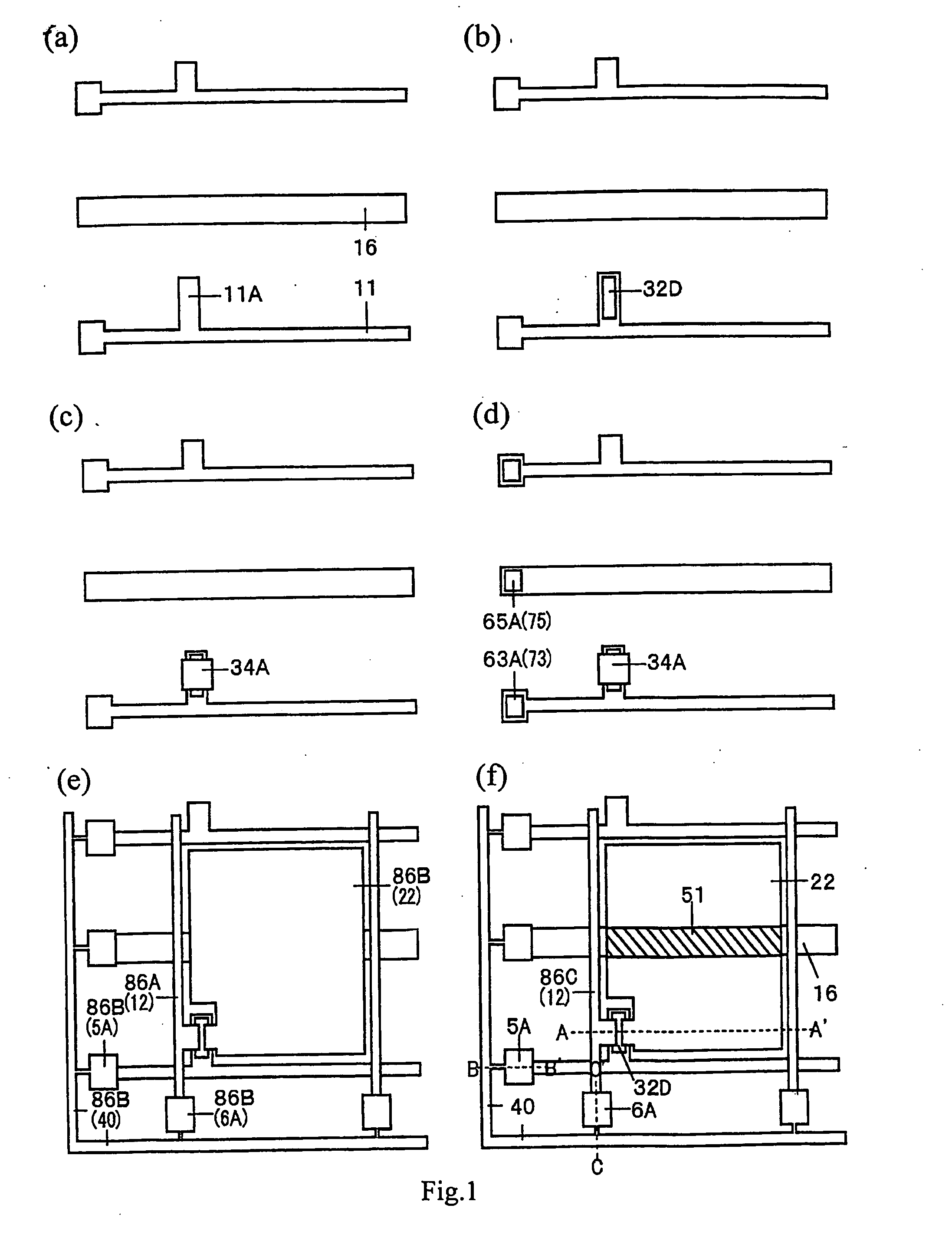
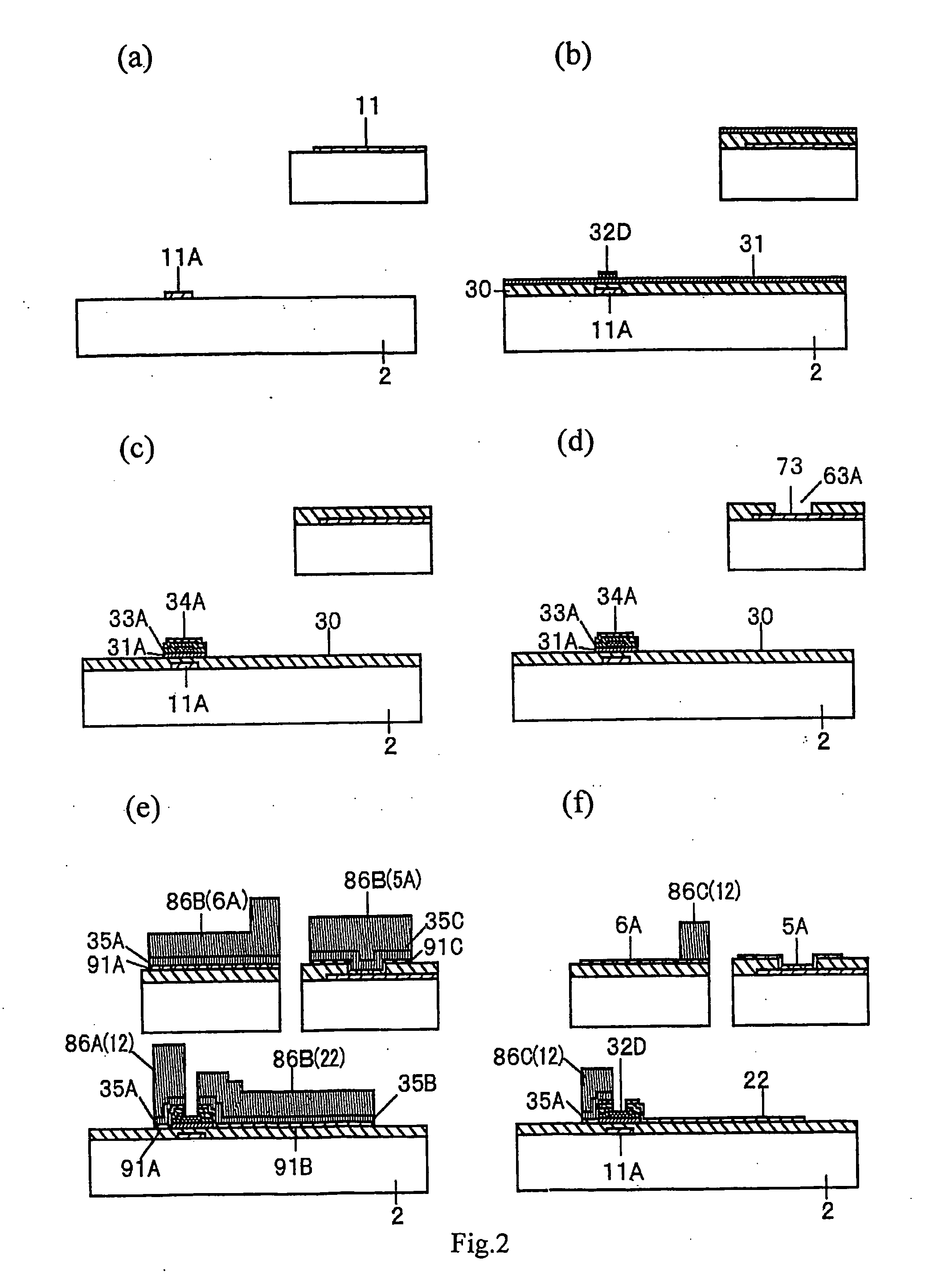
[0363] To begin with, in Embodiment 1, Cr, Ta, Mo or the like or an alloy or silicide thereof, for example, is deposited as a first metal layer about 0.1 to 0.3 μm thick on the primary surface of a glass substrate 2 using an SPT or other vacuum film depositing equipment similarly to the conventional example. It goes without saying that a laminate of Al or an Al alloy and one of these metals with a high heat resistance may be used to lower the resistance if required. Next, a scan line 11 doubling as a gate electrode 11A and a storage capacitor line 16 are selectively formed using micro-fabrication technology as shown in FIGS. 1(a) and 2(a).

[0364] Next, three thin film layers comprising a first SiNx layer 30 forming a gate insulating layer, a first amorphous silicon layer 31 forming a channel for an insulating gate type transistor containing hardly any impurities, and a second SiNx layer 32 forming an insulating layer for protecting the channel are successively deposited about 0.3, 0...

embodiment 2

[0373] In Embodiment 2, the manufacturing process is carried out identically to that in Embodiment 1 up to the formation process of the contacts 63A and 65A above the scan line 11 and the storage capacitor line 16 as shown in FIGS. 3(d) and 4(d). However, an anodizable metal is required for the heat resistant metal layer 34, and Cr. Mo, W and the like are not suitable therefor, so at least, Ti, or preferably Ta or a silicide of a metal with a high melting point may be selected.

[0374] Then, IZO or ITO, for example, is deposited as a transparent conductive layer 91 about 0.1 to 0.2 μm thick over the entire surface of the glass substrate 2 using an SPT or other vacuum film depositing equipment; an Al or Al (Nd) alloy thin film layer about 0.3 μm thick is subsequently deposited as an anodizable low resistant metal layer; using micro-fabrication technology, the Al or Al(Nd) alloy thin layer 35, the transparent conductive layer 91, the heat resistant metal layer 34A, the second amorphous...

embodiment 3

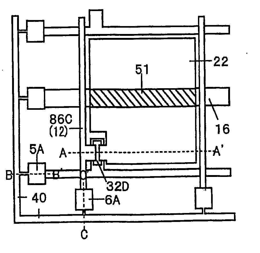
[0382] In Embodiment 3, a second SiNx layer is selectively left above a gate electrode 11A finer in width than said gate electrode to make a protective insulating layer 32D using micro-fabrication technology as shown in FIGS. 5(b) and 6(b), and the manufacturing process is carried out identically to that in Embodiment 1 up to the exposure of the first amorphous silicon layer 31.

[0383] Continuing, a second amorphous silicon layer 33 about 0.05 μm thick, for example, containing phosphorous, for example, as an impurity is deposited over the entire surface using a PCVD equipment in a similar manner. Then, a thin film layer 34 of Ti, Cr, Mo or the like, for example, is deposited as a heat resistant metal layer about 0.1 μm thick using an SPT or other vacuum film depositing equipment, and photosensitive resin patterns 81A and 81B are formed using half-tone exposure technology so as to have openings 63 and 65A at the contact formation region of the scan line 11 and the storage capacitor l...


PUM

PropertyMeasurementUnit
diagonal lengthaaaaaaaaaa
thickaaaaaaaaaa
thickaaaaaaaaaa

Abstract

When the channel length is shortened in a conventional manufacturing method with a reduced numbers of processes, the manufacturing margin is decreased, causing a lower yield. A four-mask process and a three-mask process proposal are constructed for a TN type liquid crystal display device made by combining a novel technology for streamlining the signal wire formation process and pixel electrode formation process by adopting a half-tone exposure technology, a novel technology for streamlining the electrode terminal protective layer formation process by adopting a half-tone exposure technology in a publicly known source and drain wiring anodization process, and a novel technology for streamlining the scan line formation process and the semiconductor layer formation process, the scan line formation process and the etch stop layer formation process, and the scan line formation process and the contact formation process.

Description

BACKGROUND OF THE INVENTION [0001] 1. Field of the Invention [0002] The present invention relates to a liquid crystal display device with a color image display function, and in particular to an active type liquid crystal display device. [0003] 2. Description of Related Art [0004] Television and various other image display devices that have a liquid crystal display 5 to 50 cm in diagonal length are provided on a mass production commercial base through progress in recent years in micro-fabrication technology, liquid crystal material technology, high-density packaging technology, and the like. In addition, a color display can easily be created by forming an RGB color layer on one of the two glass substrates composing a liquid crystal panel. In particular, in a so-called active liquid crystal panel with a switching element inside each pixel, there is little cross-talk, the response rate is high, and images with a high contrast ratio are guaranteed. [0005] For these liquid crystal displa...

Claims


Application Information

Patent Timeline
Patent Type & Authority Applications(United States)
IPC IPC(8): G02F1/1362G02F1/1368G09F9/30H01L21/336H01L21/768H01L29/786
CPCG02F1/1362G02F2001/136236G02F2001/136231G02F1/136231G02F1/136236
Inventor KAWASAKI, KIYOHIRO
Owner AU OPTRONICS CORP
Why Eureka
Try Eureka