Tape carrier, semiconductor apparatus, and semiconductor module apparatus

a technology of semiconductor modules and tape carriers, applied in the direction of printed circuit aspects, sustainable manufacturing/processing, final product manufacturing, etc., can solve the problems of difficulty in producing a wiring pattern with a wiring pitch smaller, insulating tapes, wiring patterns, etc., and several obstacles in realizing finer pitches and thin films

Active Publication Date: 2010-03-02
SHENZHEN TOREY MICROELECTRONIC TECH CO LTD
View PDF10 Cites 71 Cited by
  • Summary
  • Abstract
  • Description
  • Claims
  • Application Information

AI Technical Summary

Benefits of technology

[0031]The present invention is in view of the foregoing problems, and has as an object to provide a tape carrier for COF semiconductor apparatuses, a COF semiconductor apparatus, and a semiconductor module apparatus, with all of which the following defect is preventable. Specifically, in a case in which a bump electrode is displaced when bonded to a wiring pattern, the wiring pattern is prevented from coming into contact with an adjacent bump electrode to the bump electrode that is supposed to be in contact with the wiring pattern. At the same time, the wiring pattern is prevented from being disconnected or peeling off.
[0033]With this structure, the connecting section of the wiring pattern is smaller in wiring pitch than the remaining part of the overlap part, which remaining part is other than the connecting section. This makes it possible to prevent the defect that, in the case in which the bump electrode is displaced when bonded to the wiring pattern, the wiring pattern is prevented from coming into contact with an adjacent bump electrode to the bump electrode that is supposed to be in contact with the wiring pattern.
[0034]Further, with the structure, the overlap part of the wiring pattern has a greater wiring width in the remaining part of the wiring pattern, which remaining part is other than the connecting section, than in the connecting section. This makes it possible to assure, or even improve, mechanical strength and bond strength that are necessary for the wiring pattern. Thus, the wiring pattern is prevented from being disconnected or peeling off.
[0035]Accordingly, with the structure, an advantage is produced that a tape carrier for COF semiconductor apparatuses is provided, with which tape carrier the wiring pattern and the bump electrode are electrically connected in a normal manner, and at the same time, the wiring pattern is prevented from being disconnected or peeling off.

Problems solved by technology

This makes it difficult to produce a wiring pattern with a wiring pitch smaller than 45 μm.
Furthermore, insulating tapes, wiring patterns, and the like need to be thinner.
There are, however, several obstacles in realizing finer pitches and thinner films.
One of the obstacles is that, because the pitch of the wiring pattern (inner lead) is small, a defect occurs if the bump electrode of the semiconductor device is displaced when bonded to the wiring pattern (inner lead).
In other words, in a COF semiconductor apparatus with a fine wiring pitch smaller than 35 μm, if the bump electrode of the semiconductor device is displaced when bonded to the wiring pattern, the defect is likely to occur that the wiring pattern (inner lead) comes into contact with an adjacent bump electrode to the bump electrode.
This problem is more likely to occur in a COF semiconductor apparatus with a wiring pitch of 30 μm or smaller.
However, narrowing the width of the wiring pattern (inner lead) results in degrading mechanical strength of the wiring pattern and bond strength between the wiring pattern and the insulating tape.
This causes a problem that the wiring pattern is easily disconnected or easily peels off in the steps from mounting and bonding the semiconductor device to packaging the COF semiconductor apparatus into a module.
There is, however, difficulty in realizing a finer pitch while maintaining this characteristic of the COF semiconductor apparatus, that is, the COF semiconductor apparatus can be folded freely.
Specifically, folding the COF semiconductor apparatus freely causes the wiring pattern to be easily disconnected or to peel off easily.
This causes a problem that the wiring pattern 23 is disconnected or peels off.

Method used


Image

  • Tape carrier, semiconductor apparatus, and semiconductor module apparatus
  • Tape carrier, semiconductor apparatus, and semiconductor module apparatus
  • Tape carrier, semiconductor apparatus, and semiconductor module apparatus

Examples


Embodiment Construction

[0048]The following describes an embodiment of the present invention, with reference to FIGS. 1 to 4.

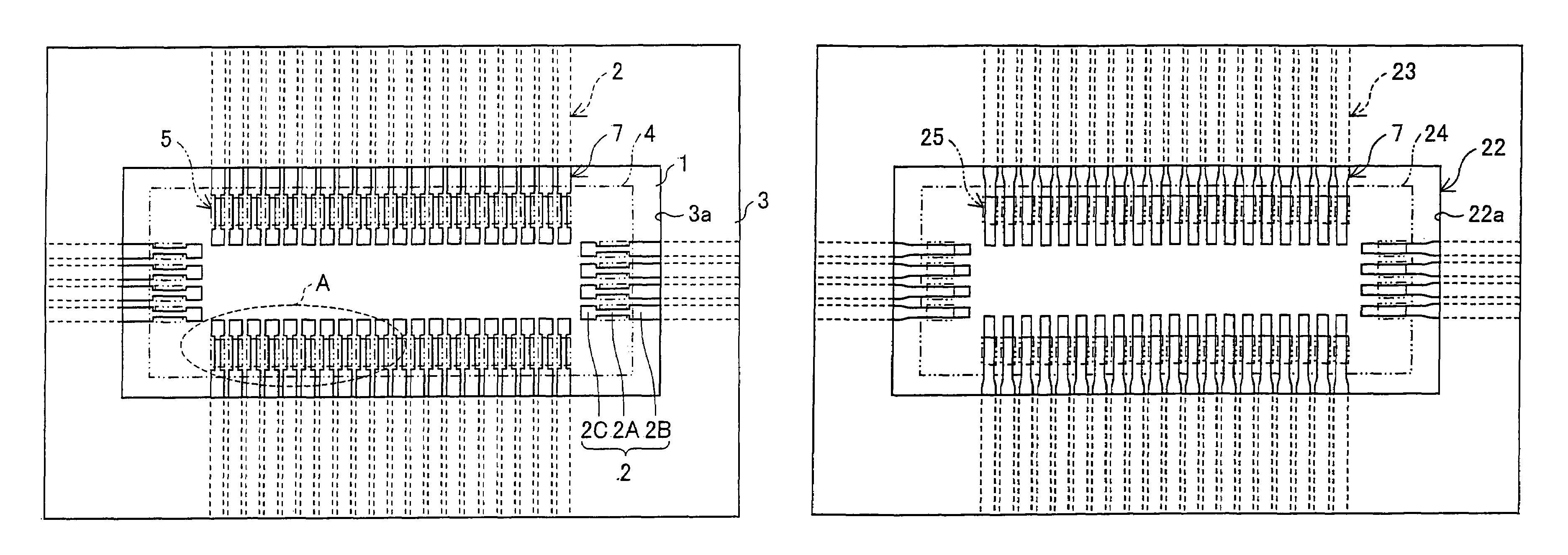
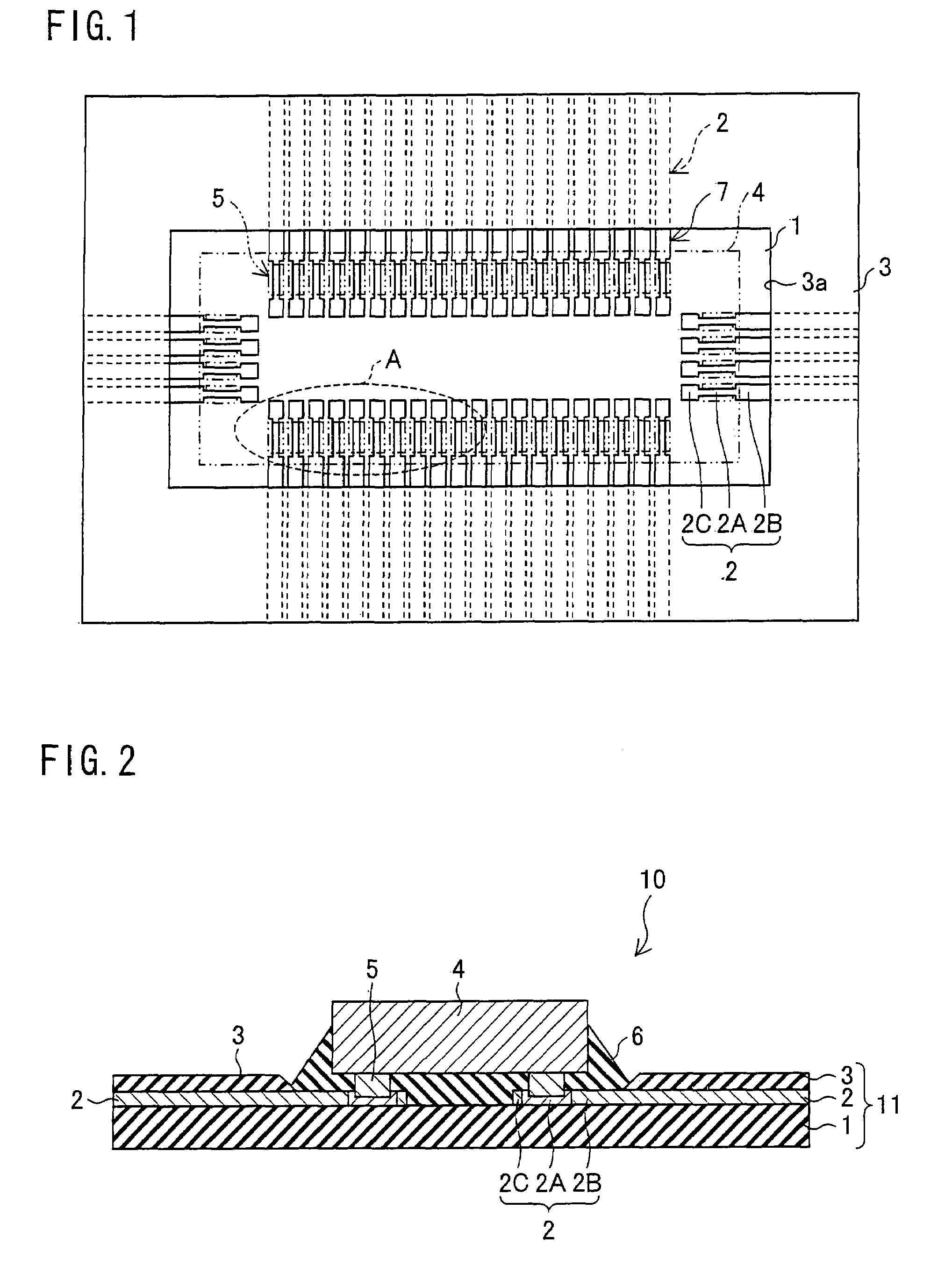
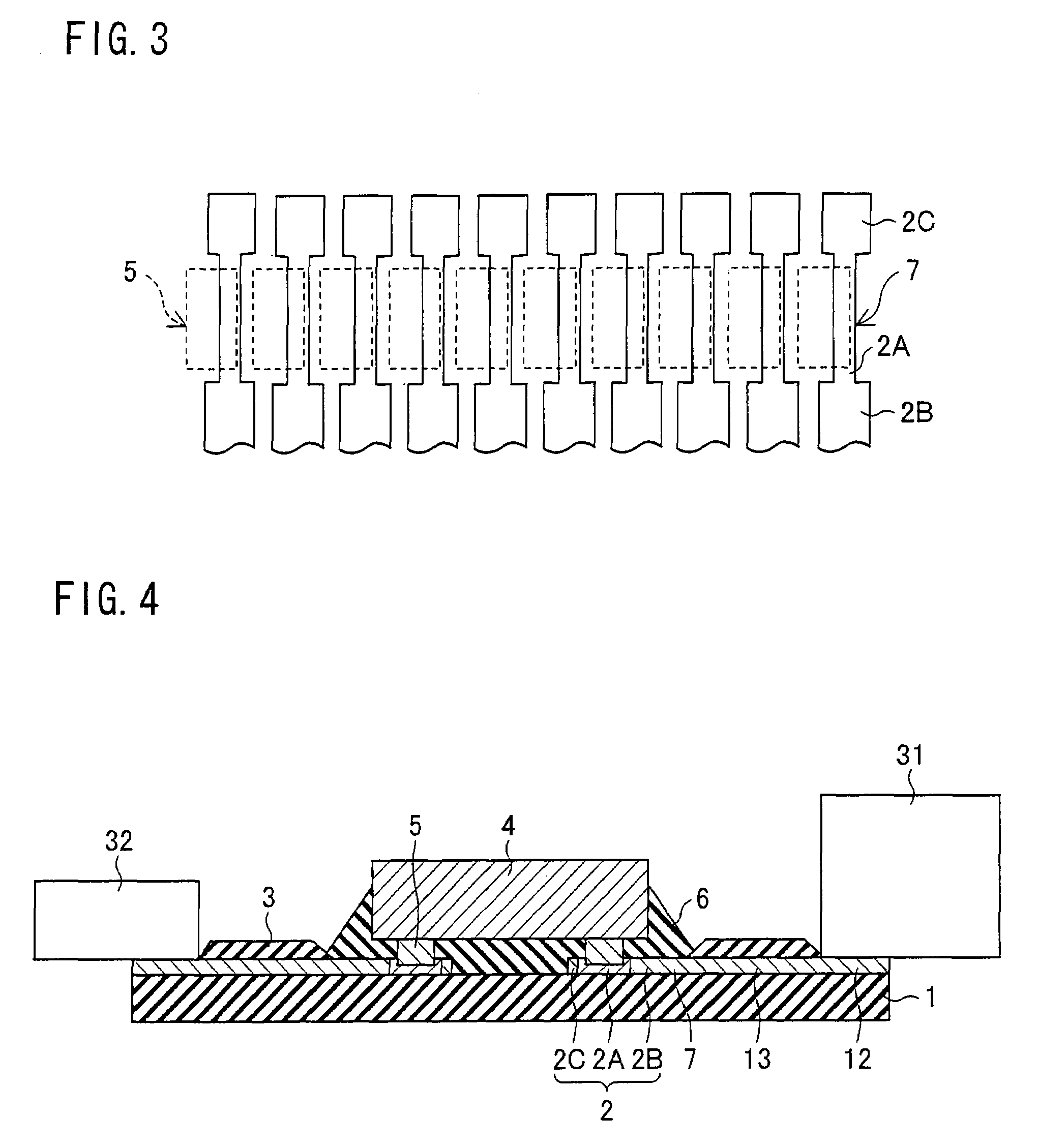
[0049]FIG. 1 is a plan view showing a schematic structure of the vicinity of a part of a COF semiconductor apparatus of the present embodiment, on which part (mount area) a semiconductor device is mounted. FIG. 2 is a sectional view showing a schematic structure of the vicinity of the part. FIG. 4 is a sectional view showing a schematic structure of a semiconductor module apparatus of the present embodiment, including the COF semiconductor apparatus shown in FIGS. 1 and 2. In FIG. 1, for convenience of description, the semiconductor device is indicated by a dashed double-dotted line, and the insulating resin is omitted.

[0050]As shown in FIGS. 1 and 2, the COF semiconductor apparatus (for convenience of description, this apparatus will be referred to simply as “semiconductor apparatus” hereinafter) 10 of the present embodiment includes a semiconductor device 4 and a tape carrier 11 (t...


PUM


Abstract

A tape carrier of the present invention includes an insulating tape and a wiring pattern formed on the insulating tape. The wiring pattern includes a connecting section via which the wiring pattern is connected to a bump electrode. The connecting section is provided at a part of an overlap part of the wiring pattern, which overlap part overlaps a semiconductor device when the semiconductor device is mounted on the wiring pattern. The connecting section of the wiring pattern is smaller in wiring width than the remaining part of the overlap part, which remaining part is other than the connecting section.

Description

[0001]This Nonprovisional application claims priority under 35 U.S.C. §119(a) on Patent Application No. 134426 / 2006 filed in Japan on May 12, 2006, the entire contents of which are hereby incorporated by reference.FIELD OF THE INVENTION[0002]The present invention relates to a tape carrier for a COF semiconductor apparatus in which a semiconductor device is mounted on and bonded to a wiring pattern by use of a chip-on-film (COF) method. The present invention also relates to a COF semiconductor apparatus using the tape carrier, and a semiconductor module apparatus using the tape carrier.BACKGROUND OF THE INVENTION[0003]TCP (Tape Carrier Package) type semiconductor apparatuses (hereinafter, “TCP semiconductor apparatus”) have conventionally been known as semiconductor apparatuses in which a semiconductor device is mounted on and coupled to a flexible printed circuit.[0004]In recent years, COF type semiconductor apparatuses (hereinafter, “COF semiconductor apparatus) have been employed....

Claims


Application Information

Patent Timeline
Patent Type & Authority Patents(United States)
IPC IPC(8): H01L23/495H01L21/50
CPCH01L21/563H01L23/49838H01L23/4985H05K1/111H01L2224/73203H01L2924/01078H01L2924/01079H05K1/189H05K2201/09727H05K2201/10674H01L2224/16225H01L2224/32225H01L2224/73204H01L2924/00H01L2224/16237Y02P70/50
Inventor SEKO, TOSHIHARU
Owner SHENZHEN TOREY MICROELECTRONIC TECH CO LTD
Why Eureka
Try Eureka