Liquid crystal display device

a liquid crystal display and display device technology, applied in non-linear optics, instruments, optics, etc., can solve the problems of light leakage, less adhesion of black matrix to substrate, etc., to prevent the peeling of layered insulating films, improve substrate-side adhesion of sealing materials, and avoid peeling of black matrix from substrate sides

Active Publication Date: 2010-04-01
PANASONIC LIQUID CRYSTAL DISPLAY CO LTD +1
View PDF7 Cites 60 Cited by
  • Summary
  • Abstract
  • Description
  • Claims
  • Application Information

AI Technical Summary

Benefits of technology

[0024]Another object of the present invention is to provide a liquid crystal display device that is improved in the substrate-side adhesion of a sealing material, that prevents the peeling of layered insulating films interposed between the sealing material and a substrate, and that is capable of protecting wiring or a circuit that is formed below the insulating films from a mechanical impact.
[0025]In a liquid crystal display device according to an aspect of the present invention, stress that concentrates when a sealing material is cured is dispersed by concave and convex portions formed on the sealing material side of a black matrix (the concave portion has a depth that is less than the thickness of the light-shielding film, in other words, the concave portion does not pass through the light-shielding film), to thereby reduce a force that acts to peel the black matrix off from a substrate. With this, the peeling of the black matrix from the substrate side can be avoided without forming a so-called through hole in the black matrix. In a liquid crystal display device according to another aspect of the present invention, an insulating film that extends to the sealing material formation region includes an inorganic insulating film placed on the front side, which is closer to the sealing material, and an organic insulating film placed below the inorganic insulating film brought into contact with the inorganic insulating film, and a recessed portion whose depth is set such that the inorganic insulating film is passed through but the organic insulating film is not is formed along the circumferential direction of the sealing material formation region.

Problems solved by technology

The resultant problem is that the adhesion of the black matrix to the substrate is lessened.
For that reason, the part of the black matrix that overlaps with the sealing material cannot block light sufficiently, allowing light emitted from a backlight, which is placed behind the liquid crystal display panel, to transmit through the sealing material and its vicinity, and thereby causing a problem of light leakage.

Method used


Image

  • Liquid crystal display device
  • Liquid crystal display device
  • Liquid crystal display device

Examples


first embodiment

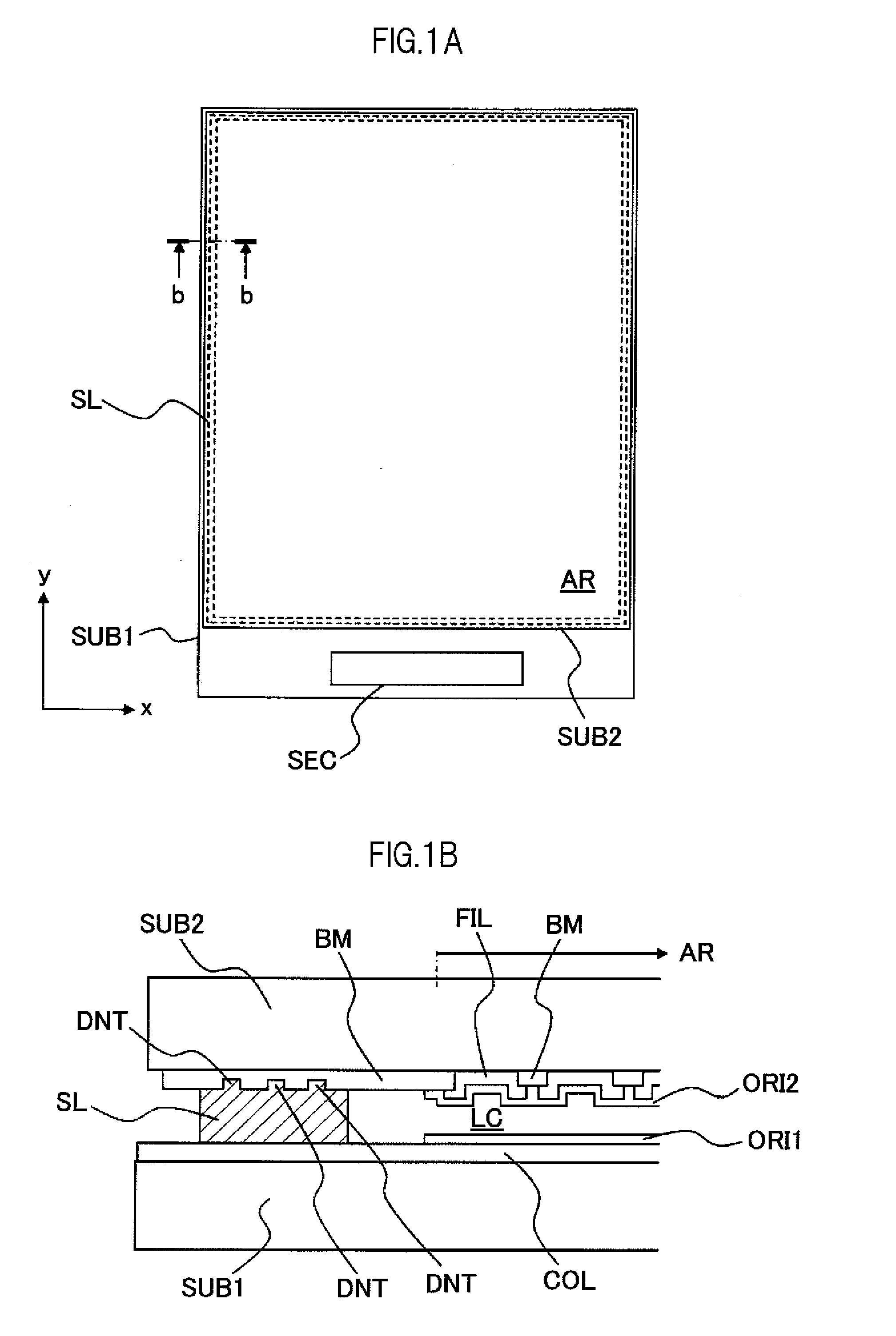
[0066]FIGS. 1A and 1B are schematic structural diagrams illustrating a liquid crystal display device according to a first embodiment of the present invention. FIG. 1A illustrates a plan view and FIG. 1B illustrates a sectional view taken along the line b-b of FIG. 1A. The liquid crystal display device illustrated in FIGS. 1A and 1B is, for example, a liquid crystal display device for a cellular phone.

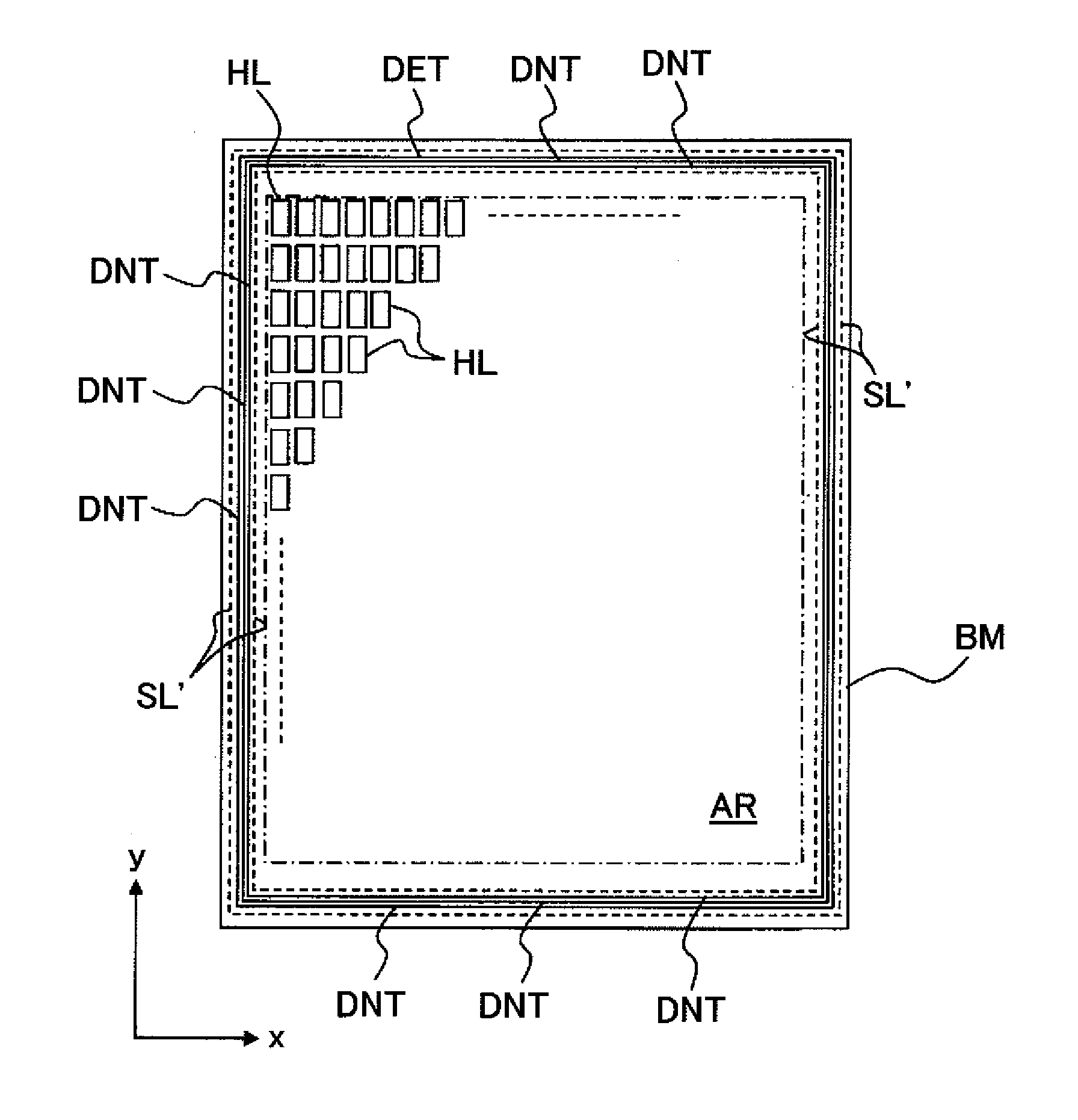
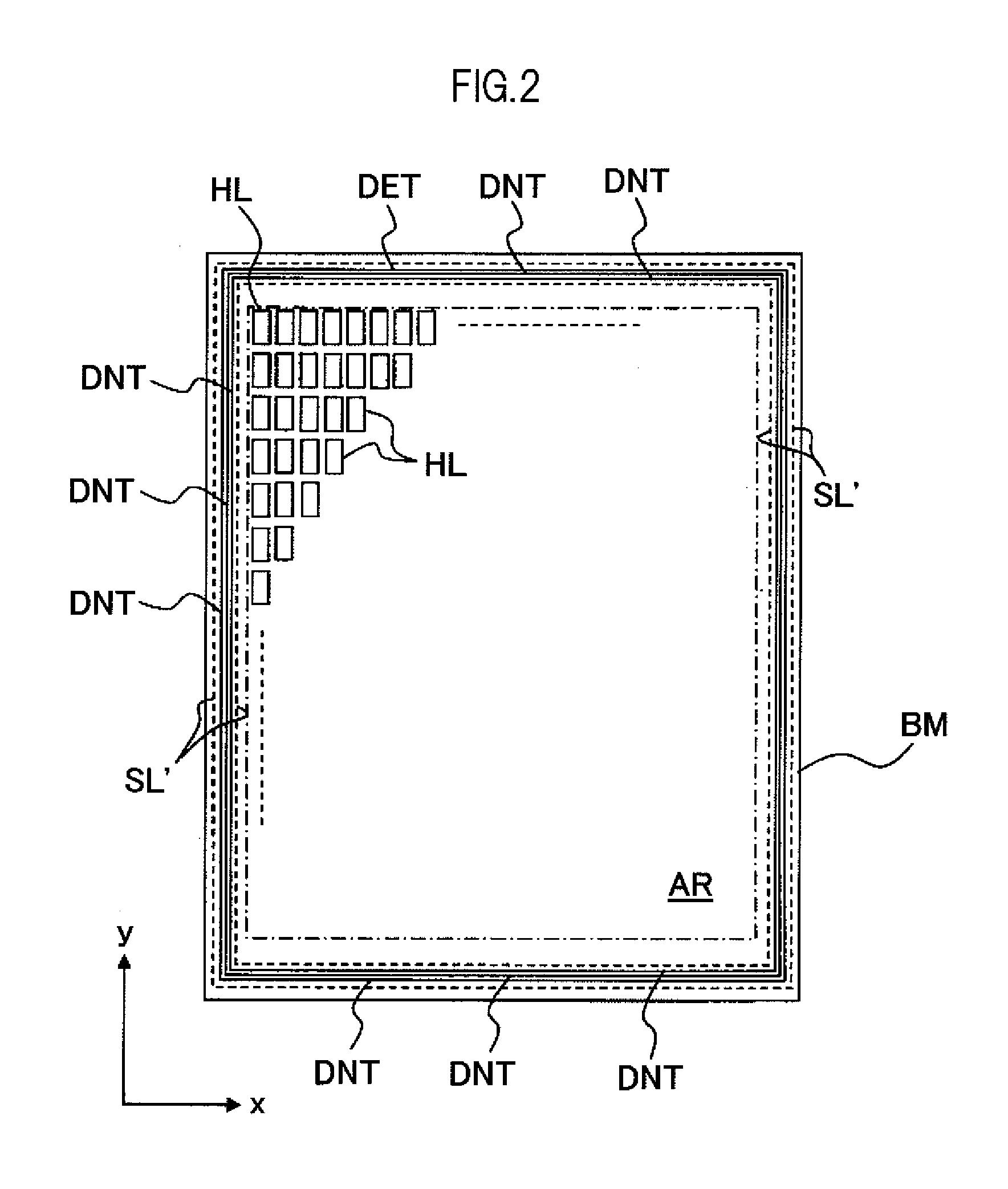
[0067]In FIG. 1A, a substrate SUB1 and a substrate SUB2 which are made of, for example, glass are arranged so as to be opposed to each other. The substrate SUB2 is smaller in area than the substrate SUB1, and arranged such that one of the four sides of the substrate SUB1, for example, the lower side in the drawing, is exposed. Along the lower side of the substrate SUB1 in the drawing, a semiconductor device (chip) SEC for driving pixels is mounted face down.

[0068]A liquid crystal LC (see FIG. 1B) is sandwiched between the substrate SUB1 and the substrate SUB2. The liquid crystal LC is s...

second embodiment

[0082]FIG. 4 is a schematic sectional view illustrating a liquid crystal display device according to a second embodiment of the present invention, and is drawn in a manner that corresponds to FIG. 1B.

[0083]FIG. 4 differs from FIG. 1B in that an overcoat film OC is formed on the liquid crystal side of the substrate SUB2 to cover the black matrix BM and the color filter FIL. The overcoat film OC is formed when, for example, the liquid crystal LC side of the substrate SUB2 is to be leveled. The overcoat film OC is, for example, a resin layer formed by application.

[0084]The overcoat film OC also covers a region of the black matrix BM where the recessed portions DNT are formed, and the sealing material SL provided so as to be opposed to this region for forming the recessed portions DNT abuts the overcoat film OC. In other words, the overcoat film OC is interposed between the black matrix BM and the sealing material SL. In addition, in the second embodiment, the overcoat film OC is formed...

third embodiment

[0086]FIG. 5 is a schematic sectional view illustrating a liquid crystal display device according to a third embodiment of the present invention, and is drawn in a manner that corresponds to FIG. 4.

[0087]FIG. 5 differs from FIG. 4 in that the overcoat film OC is formed relatively thin so that a part of the overcoat film OC that covers the recessed portions DNT of the black matrix BM has surface irregularities reflecting the recessed portions DNT. Recessed portions (denoted by reference symbol DNT2 in FIG. 5) are thus formed in the overcoat film OC in places that coincide with the recessed portions DNT. The rest of the liquid crystal display device according to the third embodiment is substantially the same as in the second embodiment, and descriptions on the similar points are omitted.

[0088]In the thus structured liquid crystal display device, too, a concave-convex surface is formed at the interface between the sealing material SL and the overcoat film OC along a force transmission ...


PUM

PropertyMeasurementUnit
widthaaaaaaaaaa
thicknessaaaaaaaaaa
thicknessaaaaaaaaaa

Abstract

Provided is a liquid crystal display device including: a first substrate and a second substrate which are arranged so as to be opposed to each other for sandwiching a liquid crystal; an image display portion; a sealing material which seals the liquid crystal; and a light-shielding film which is formed on a liquid crystal side of the second substrate so that a part of the light-shielding film extends beyond the image display portion to overlap with the sealing material, and which has openings in the image display portion, at least in regions of the multiple pixels, in which the part of the light-shielding film that overlaps with the sealing material has a recessed portion formed on a sealing material side of the light-shielding film continuously or discontinuously along a circumferential direction of the sealing material, to a depth that is smaller than a thickness of the light-shielding film.

Description

CROSS-REFERENCE TO RELATED APPLICATIONS[0001]The present application claims priority from Japanese applications JP 2008-255939 filed on Oct. 1, 2008, and JP 2008-263465 filed on Oct. 10, 2008, the contents of which are hereby incorporated by reference into this application.BACKGROUND OF THE INVENTION[0002]1. Field of the Invention[0003]The present invention relates to a liquid crystal display device, and more particularly, to a liquid crystal display device in which a pair of substrates sandwiching a liquid crystal is bonded together by a sealing material for sealing the liquid crystal.[0004]2. Description of the Related Art[0005]Liquid crystal display devices (liquid crystal display panels) have a structure in which a pair of substrates arranged so as to be opposed to each other for sandwiching a liquid crystal serves as an envelope, an image display portion including an aggregation of multiple pixels is located in a direction in which the liquid crystal spreads, and the liquid cry...

Claims


Application Information

Patent Timeline
Patent Type & Authority Applications(United States)
IPC IPC(8): G02F1/1339
CPCG02F1/133512G02F2001/133388G02F1/1339G02F1/133388
Inventor SEKIYA, KUNINOBUYAMADA, YASUYUKI
Owner PANASONIC LIQUID CRYSTAL DISPLAY CO LTD
Why Eureka
Try Eureka