Semiconductor element, method of manufacturing semiconductor element, multi-layer printed circuit board, and method of manufacturing multi-layer printed circuit board

a technology of semiconductor elements and printed circuit boards, which is applied in the direction of printed circuit parts, printed circuit non-printed electric components association, fixed connections, etc., can solve the problems of resin residue on the pad, possible burning of aluminum pads, and discoloration of pads, so as to prevent peeling and cracking, prevent the detachment and position error of solder bumps, and improve the adhesion between the substrate and the semiconductor devi

Inactive Publication Date: 2007-09-13
IBIDEN CO LTD
View PDF57 Cites 59 Cited by
  • Summary
  • Abstract
  • Description
  • Claims
  • Application Information

AI Technical Summary

Benefits of technology

[0059] According to the invention recited in claim 43, by filling the resin filling material between the recess or the through hole of the substrate and the semiconductor device, the adhesion between the substrate and the semiconductor device can be improved. In addition, to relax a stress generated by thermal expansion, this resin filling material can prevent the cracking of the core substrate and the waviness of the interlayer resin insulating layer and the solder resist layer. Due to this, it is possible to prevent peeling and cracking from occurring to the surrounding of the solder bump or the like. Accordingly, it is possible to prevent the detachment and positional error of the solder bump and to, therefore, improve electrical connection characteristics and reliability. As the resin filling material, a thermosetting resin, a thermoplastic resin or a mixture thereof can be used.

Problems solved by technology

Besides, the pad is discolored due to the adhesion of a development solution.
On the other hand, if via holes are formed by laser, there is a possibility of burning the aluminum pad.
Also, if via holes are formed under the conditions that the pad is not burned, a resin residue on the pad occurs.
As a result, a positional error and a connection defect tend to occur.

Method used


Image

  • Semiconductor element, method of manufacturing semiconductor element, multi-layer printed circuit board, and method of manufacturing multi-layer printed circuit board
  • Semiconductor element, method of manufacturing semiconductor element, multi-layer printed circuit board, and method of manufacturing multi-layer printed circuit board
  • Semiconductor element, method of manufacturing semiconductor element, multi-layer printed circuit board, and method of manufacturing multi-layer printed circuit board

Examples


third modification

of First Embodiment

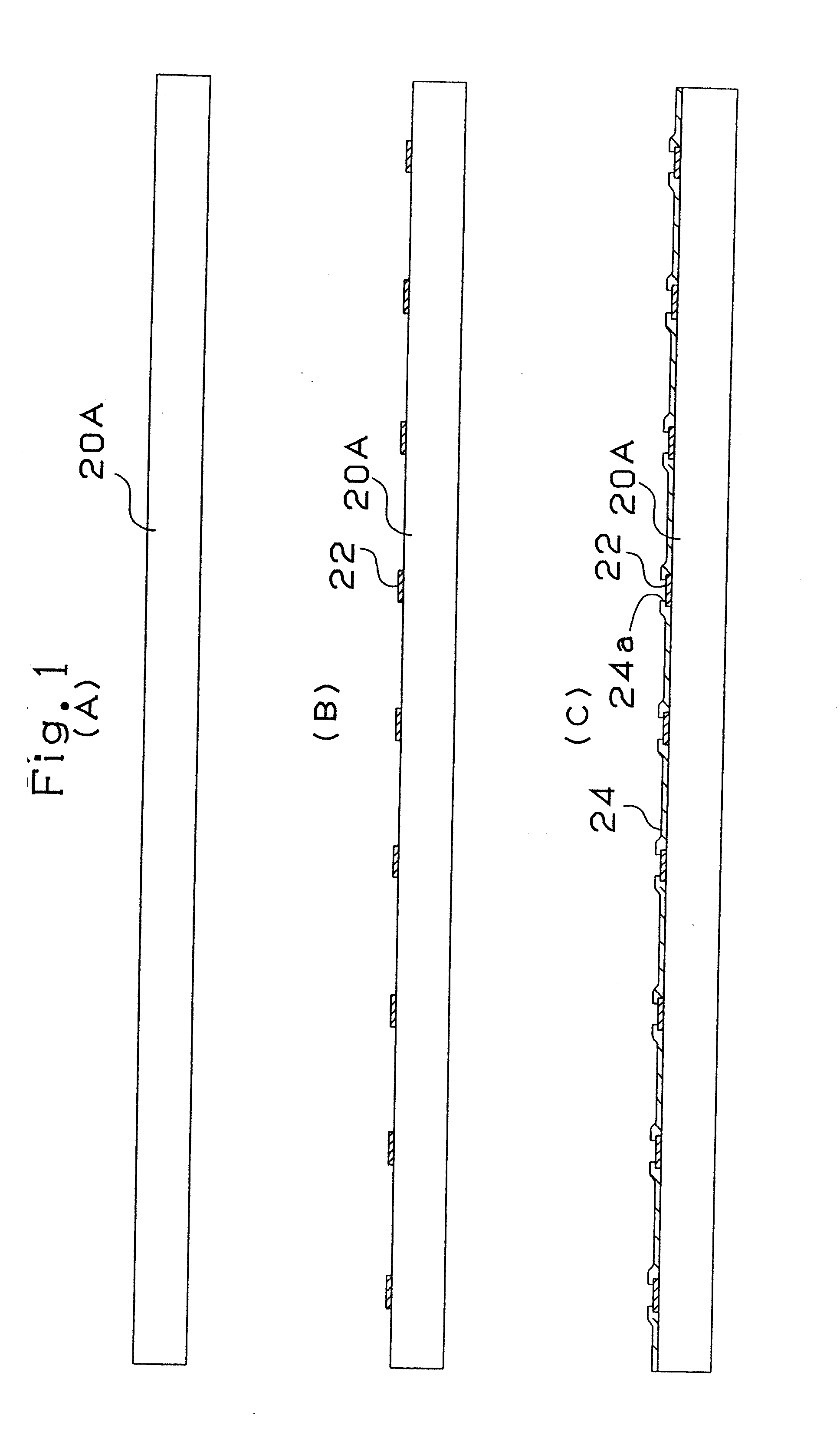
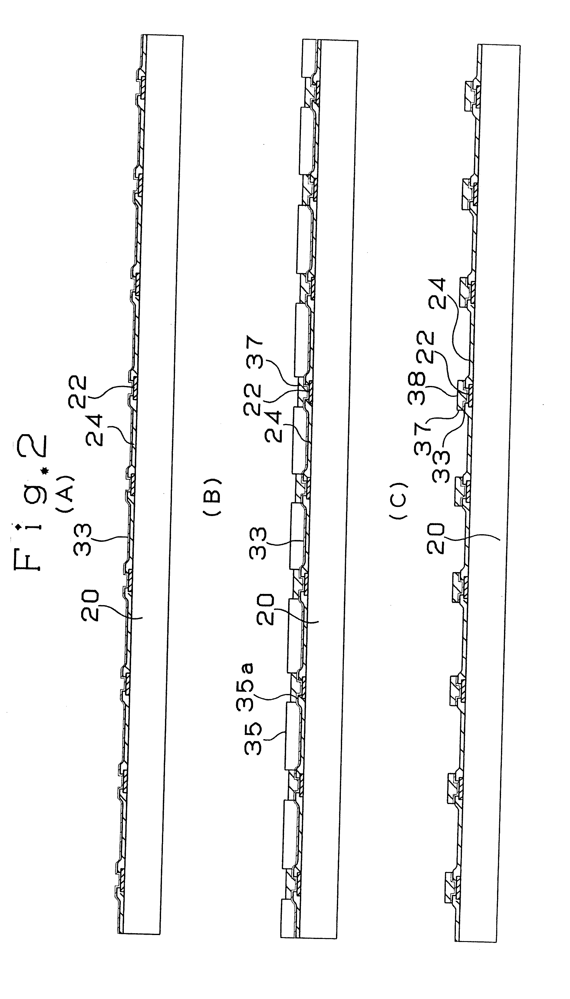
[0165] The method of manufacturing a semiconductor device 20 according to the third modification will be described with reference to FIG. 9. In case of the semiconductor device according to the second modification stated above with reference to FIG. 8, each transition layer 38 has a two-layer structure comprising the thin film layer 33 and the thickening layer 37. In the third modification, as shown FIG. 9(D), by contrast, a transition layer 38 is constituted to have a three-layer structure comprising the first thin film layer 33, the second thin film layer 36 and a thickening layer 37.

[0166] The manufacturing method in the third modification will be described with reference to FIG. 9.

[0167] (1) As in the case of the first modification in the first embodiment stated above with reference to FIG. 6(A), the second thin film layer 36 is built up on the first thin film layer 33 by sputtering, deposition or electroless plating (see FIG. 9(A)). Metal to be built up in ...

first embodiment

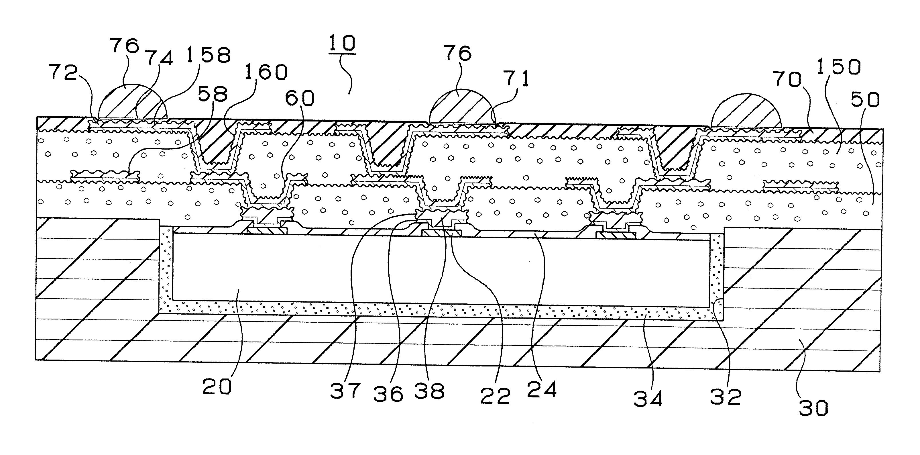
[0177] As shown in FIG. 14, the multilayer printed circuit board 10 comprises a core substrate 30 containing therein an IC chip 20, an interlayer resin insulating layer 50 and an interlayer resin insulating layer 150. Via holes 60 and conductor circuits 58 are formed on the interlayer resin insulating layer 50. Via holes 160 and conductor circuits 158 are formed on the interlayer resin insulating layer 150.

[0178] A solder resist layer 70 is provided on the interlayer resin insulating layer 150. Solder bumps 76 for connecting to an external substrate such as a daughter board or a mother board, which is not shown in FIG. 14, are provided on the conductor circuits 158 under the openings 71 of the solder resist layer 70, respectively.

[0179] In the multilayer printed circuit board 10 in this embodiment, the IC chip 20 is integrated into the core substrate 30 and transition layers 38 are provided on the respective pads 22 of the IC chip 20. Due to this, it is possible to electrically co...

second embodiment

[0235] The second embodiment of the present invention will be described hereinafter with reference to the drawings.

[0236] The constitution of a multilayer printed circuit board containing therein a semiconductor device (or an IC chip) 20 in the second embodiment will be described.

[0237] As shown in FIG. 24, the multilayer printed circuit board 10 comprises a heat sink 30D on which the IC chip 20 in the first embodiment stated above with reference to FIG. 3(B) is mounted, a core substrate 31 containing therein the IC chip 20, an interlayer resin insulating layer 50 and an interlayer resin insulating layer 150. Via holes 60 and conductor circuits 58 are formed on the interlayer resin insulating layer 50. Via holes 160 and conductor circuits 158 are formed on the interlayer resin insulating layer 150.

[0238] A solder resist layer 70 is provided on the interlayer resin insulating layer 150. Solder bumps 76 for connecting to an external substrate such as a daughter board or a mother bo...


PUM


Abstract

A transition layer 38 is provided on a die pad 22 of an IC chip 20 and integrated into a multilayer printed circuit board 10. Due to this, it is possible to electrically connect the IC chip 20 to the multilayer printed circuit board 10 without using lead members and a sealing resin. Also, by providing the transition layer 38 made of copper on an aluminum pad 24, it is possible to prevent a resin residue on the pad 24 and to improve connection characteristics between the die pad 24 and a via hole 60 and reliability.

Description

CROSS-REFERENCE TO RELATED APPLICATIONS [0001] This application is a Divisional of and claims the benefit of priority under 35 U.S.C. §120 from U.S. Ser. No. 10 / 380,631, filed Mar. 21, 2003 which is the National Stage of PCT / JP01 / 03589 filed Apr. 25, 2001 and claims the benefit of priority under 35 U.S.C. § 119 from Japanese Patent Application priority documents, 2000-290231 filed in Japan on Sep. 25, 2000; 2000-290232 filed in Japan on Sep. 25, 2000; 2000-382806 filed in Japan on Dec. 15, 2000; 2000-382807 filed in Japan on Dec. 15, 2000; 1000-382813 filed in Japan on Dec. 15, 2000; and 2000-382814 filed in Japan on Dec. 15, 2000.TECHNICAL FIELD OF THE INVENTION [0002] The present invention relates to a semiconductor device such as an IC chip, a semiconductor device manufacturing method, a multilayer printed circuit board into which a semiconductor device is integrated and a multilayer printed circuit board manufacturing method. BACKGROUND OF THE INVENTION [0003] An IC chip is elec...

Claims


Application Information

Patent Timeline
Patent Type & Authority Applications(United States)
IPC IPC(8): H01R12/06H01L21/301H05K3/46H01L21/60H01L23/498H01L23/538H01R12/51H05K1/18
CPCH01L21/568H01L21/6835H01L23/49811H01L23/49816H01L23/49894H01L23/5389H01L24/19H01L24/24H01L24/97H01L2224/04105H01L2224/1147H01L2224/20H01L2224/24227H01L2224/274H01L2224/97H01L2924/01004H01L2924/01005H01L2924/01011H01L2924/01012H01L2924/01013H01L2924/01015H01L2924/01018H01L2924/0102H01L2924/01027H01L2924/01029H01L2924/0103H01L2924/01033H01L2924/01039H01L2924/01046H01L2924/01047H01L2924/01051H01L2924/01074H01L2924/01078H01L2924/01079H01L2924/01082H01L2924/14H01L2924/15153H01L2924/1517H01L2924/15174H01L2924/15311H01L2924/15312H01L2924/1532H01L2924/30107H05K1/185H05K3/4602H05K2201/09036H05K2201/09563H05K2201/096H01L2924/01006H01L2924/01019H01L2924/01024H01L24/27H01L2224/73267H01L2224/12105H01L2224/24137H01L2224/32225H01L2224/32245H01L2224/92244H01L2224/0401Y10T29/49155Y10T29/49126Y10T29/4913Y10T29/49139Y10T29/49144Y10T29/49165Y10T29/49128Y10T29/49133H01L2224/82H01L2924/3512H01L2924/00H01L2924/15787H01L2924/12042H01L2224/45144H01L2224/94H01L2924/3511Y10T29/49124Y10T29/49146H01L2224/03H01L23/525H01L23/49822H01L23/49838H01L23/49866
Inventor SAKAMOTO, HAJIMEWANG, DONGDONG
Owner IBIDEN CO LTD
Why Eureka
Try Eureka