Pixel structure, display panel, eletro-optical apparatus, and method thererof

Active Publication Date: 2009-06-18
AU OPTRONICS CORP
View PDF12 Cites 61 Cited by
  • Summary
  • Abstract
  • Description
  • Claims
  • Application Information

AI Technical Summary

Benefits of technology

[0014]The present invention is further directed to a method of manufacturing a display panel, in which a method of manufacturing a pixel structure is able to prevent a metal layer made of copper, a copper alloy, or a combination thereof from being peeled off.
[0015]

Problems solved by technology

Since copper is not able to form a self-protective oxidation layer under an atmospheric environment, the copper lines are likely to be oxidized and corroded in a conventional manufacturing process of a pixel structure having the copper lines.
In addition, the TFTs using copper as the electrodes are often deteriorated due to certain properties of copper.
For instance, an adhesion between a copper electrode and a substrate is relatively unsatisfac

Method used


Image

  • Pixel structure, display panel, eletro-optical apparatus, and method thererof
  • Pixel structure, display panel, eletro-optical apparatus, and method thererof
  • Pixel structure, display panel, eletro-optical apparatus, and method thererof

Examples


Example

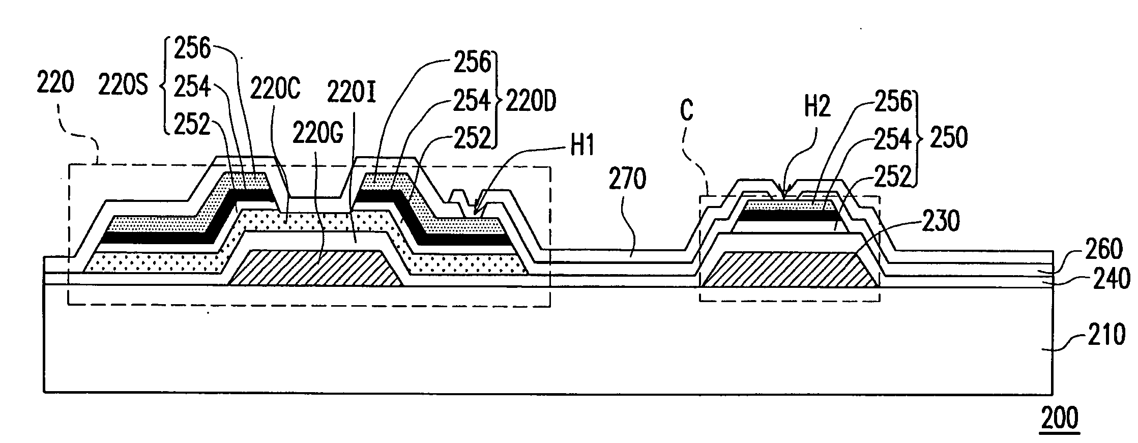
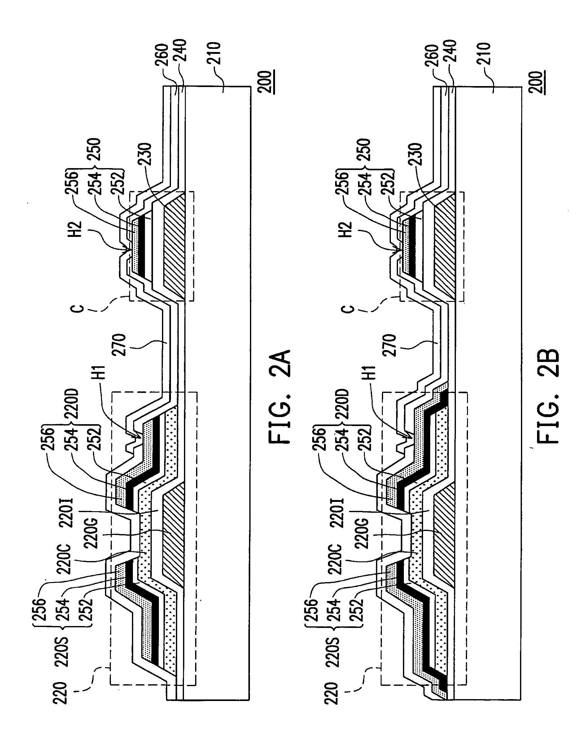
[0036]FIG. 2A is a schematic view illustrating a pixel structure according to the present invention. Referring to FIG. 2A, a pixel structure 200 disposed on a substrate 210 includes a TFT 220, a bottom capacitor electrode 230, a dielectric layer 240, an upper capacitor electrode 250, a passivation layer 260, and a pixel electrode 270. The TFT 220 and the bottom capacitor electrode 230 are disposed on the substrate 210. The passivation layer 260 covers the TFT 220 and the upper capacitor electrode 250 and has at least a first opening H1 exposing a drain 220D. The pixel electrode 270 is electrically connected to the TFT 220 through the first opening H1. Besides, in the present embodiment, the passivation layer 260 preferably has at least a second opening H2 exposing the upper capacitor electrode 250, and the pixel electrode 270 is electrically connected to the upper capacitor electrode 250 through the second opening H2, which is not limited in the present invention. Alternatively, the...


PUM


Abstract

A pixel structure disposed on a substrate including a thin film transistor (TFT), a bottom capacitor electrode, a dielectric layer, an upper capacitor electrode, a passivation layer, and a pixel electrode is provided. The TFT having a source/drain and the bottom capacitor electrode are disposed on the substrate. The dielectric layer is disposed on the bottom capacitor electrode. The upper capacitor electrode has a semiconductor layer, a barrier layer, and a metal layer. The semiconductor layer is disposed on the dielectric layer above the bottom capacitor electrode. The barrier layer is disposed on the semiconductor layer. The metal layer whose material includes copper, a copper alloy, or a combination thereof is disposed on the barrier layer. The passivation layer covers the TFT and the upper capacitor electrode and has a first opening exposing the source/drain. The pixel electrode is electrically connected to the TFT through the first opening.

Description

CROSS-REFERENCE TO RELATED APPLICATION[0001]This application claims the priority benefit of Taiwan application serial no. 96148199, filed on Dec. 17, 2007. The entirety the above-mentioned patent application is hereby incorporated by reference herein and made a part of specification.BACKGROUND OF THE INVENTION[0002]1. Field of the Invention[0003]The present invention generally relates to a display apparatus, and more particularly, to a liquid crystal display (LCD) apparatus having copper electrodes.[0004]2. Description of Related Art[0005]The rapid development of a multimedia society mostly results from the fact that semiconductor elements or human-information display apparatuses have progressed by leaps and bounds. Among the display apparatuses, flat panel displays featuring superior characteristics of high definition, great space utilization, low power consumption, and non-radiation have gradually become mainstream products in the market. At this current stage, a thin film transis...

Claims


Application Information

Patent Timeline
IPC IPC(8): H01J7/44H01L21/04H01J9/00
CPCH01L29/458H01L27/124H01L27/1255
Inventor CHEN, PO-LINLIN, CHUN-NANWU, SHU-FENGTSAI, WEN-CHING
Owner AU OPTRONICS CORP
Why Eureka
Try Eureka