Wafer level package and method of manufacturing the same and method of reusing chip

a technology of wafer level and packaging, which is applied in the direction of electrical equipment, semiconductor devices, semiconductor/solid-state device details, etc., can solve the problems of waste of packaging costs, waste of packaging time, and cost the same as the good chip to package the bad chip, so as to improve the production yield of wafer level and reduce manufacturing costs

Active Publication Date: 2010-06-03
SAMSUNG ELECTRO MECHANICS CO LTD
View PDF15 Cites 66 Cited by
  • Summary
  • Abstract
  • Description
  • Claims
  • Application Information

AI Technical Summary

Benefits of technology

[0009]The present invention has been proposed in order to solve the above-described problems, and it is, therefore, an object of the present invention to provide a wafer level package and a method of manufacturing the same and a method of reusing a chip capable of improving production yield of the wafer level package and reducing manufacturing cost thereof by selecting only a good chip to manufacture the package and reusing the good chip by removing KMPR coated on the good chip if necessary.

Problems solved by technology

Therefore, a conventional package manufacturing method in which the packaging process must be performed for each chip has a problem that it takes too long time to package all the chips in consideration of the number of the chips obtained from one wafer.
However, in the conventional wafer level package, since all of good and bad chips are packaged in a wafer level and then diced into the individual packages without selecting and packaging only the good chip, it costs the same as the good chip to package the bad chip in a FAB process.
Therefore, there have been problems such as a waste of packaging cost and reduction of production yield.

Method used


Image

  • Wafer level package and method of manufacturing the same and method of reusing chip
  • Wafer level package and method of manufacturing the same and method of reusing chip
  • Wafer level package and method of manufacturing the same and method of reusing chip

Examples


Embodiment Construction

[0029]Reference will now be made in detail to the embodiments of the present general inventive concept, examples of which are illustrated in the accompanying drawings, wherein like reference numerals refer to like elements throughout. The embodiments are described below in order to explain the present general inventive concept by referring to the figures.

[0030]First, a wafer level package in accordance with an embodiment of the present invention will be described in detail with reference to FIG. 1.

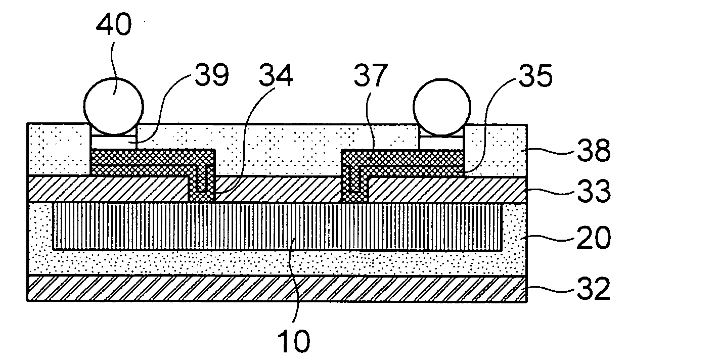
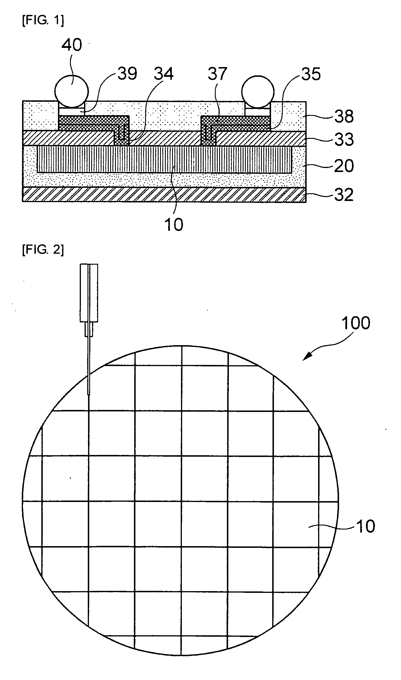
[0031]FIG. 1 is a cross-sectional view illustrating a structure of the wafer level package in accordance with the embodiment of the present invention.

[0032]As shown in FIG. 1, the wafer level package in accordance with the embodiment of the present invention includes a chip 10, a removable resin layer 20 formed to surround side surfaces and a lower surface of the chip 10, a molding material 32 formed on the lower surface of the removable resin layer 20, a dielectric layer 33 formed over th...


PUM


Abstract

The present invention relates to a wafer level package and a method of manufacturing the same and a method of reusing a chip and provides a wafer level package including a chip; a removable resin layer formed to surround side surfaces and a lower surface of the chip; a molding material formed on the lower surface of the removable resin layer; a dielectric layer formed over the removable resin layer including the chip and having via holes to expose portions of the chip; redistribution lines formed on the dielectric layer including insides of the via holes to be connected to the chip; and a solder resist layer formed on the dielectric layer to expose portions of the redistribution lines. Also, the present invention provides a method of manufacturing a wafer level package and a method of reusing a chip.

Description

CROSS-REFERENCE TO RELATED APPLICATIONS[0001]This application claims the benefit of Korean Patent Application No. 10-2008-0121660 filed with the Korea Intellectual Property Office on Dec. 3, 2008, the disclosure of which is incorporated herein by reference.BACKGROUND OF THE INVENTION[0002]1. Field of the Invention[0003]The present invention relates to a wafer level package and a method of manufacturing the same and a method of reusing a chip, and more particularly, to a wafer level package and a method of manufacturing the same and a method of reusing a chip capable of manufacturing the package by selecting only a good chip coated with KMPR and reusing the good chip by removing the KMPR coated on the good chip if necessary after dicing a wafer into the individual packages.[0004]2. Description of the Related Art[0005]A conventional package has been manufactured in such a way of cutting a wafer including a plurality of chips along dicing lines to separate the wafer into the individual...

Claims


Application Information

Patent Timeline
Patent Type & Authority Applications(United States)
IPC IPC(8): H01L23/498H01L21/78
CPCH01L21/56H01L2924/014H01L23/3114H01L24/19H01L24/97H01L2224/04105H01L2224/20H01L2224/97H01L2924/01029H01L2924/01075H01L2924/01078H01L21/568H01L2924/01033H01L2924/01005H01L2224/82H01L2924/181H01L2224/12105H01L2224/96H01L23/12H01L23/48
Inventor KANG, JOON SEOKYI, SUNGKWEON, YOUNG DO
Owner SAMSUNG ELECTRO MECHANICS CO LTD
Why Eureka
Try Eureka