

Chip package with coplanarity controlling feature
a coplanarity control and chip technology, applied in the field of integrated circuit chip packaging, can solve the problems of poor coplanarity poor reliability of the bottom chip package, and high yield loss, and achieve the effect of improving drawing legibility
- Summary
- Abstract
- Description
- Claims
- Application Information
AI Technical Summary
Benefits of technology
Problems solved by technology
Method used
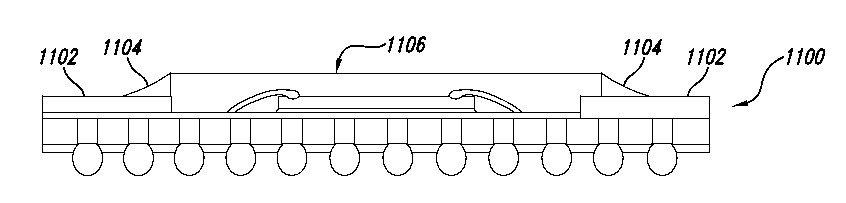
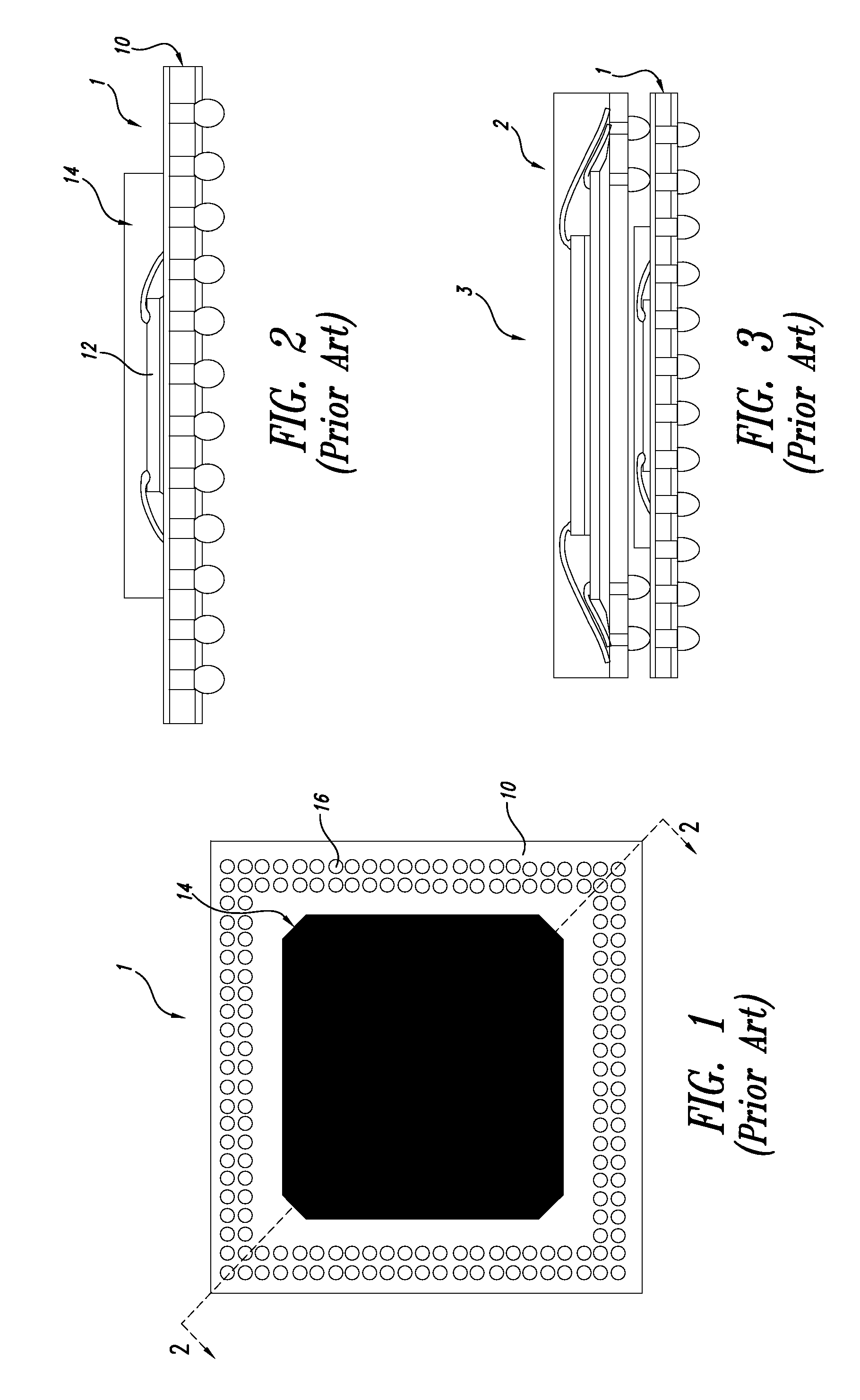
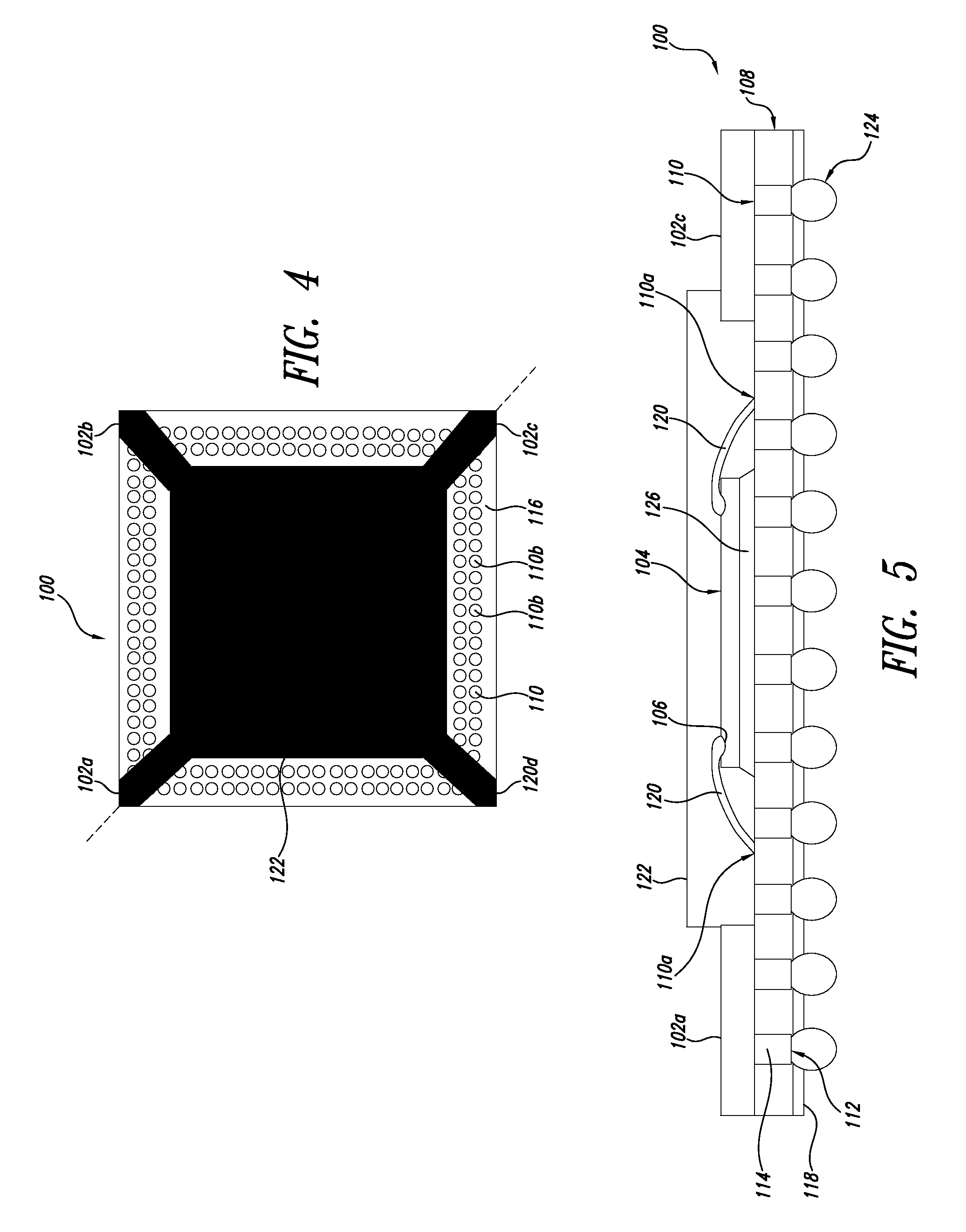
Image

Examples
Embodiment Construction
[0023]In the following description, certain specific details are set forth in order to provide a thorough understanding of various disclosed embodiments. However, one skilled in the relevant art will recognize that embodiments may be practiced without one or more of these specific details, or with other methods, components, materials, etc. In other instances, well-known structures and methods associated with integrated circuits and semiconductor manufacturing / packaging processes have not been shown or described in detail to avoid unnecessarily obscuring descriptions of the embodiments.
[0024]Unless the context requires otherwise, throughout the specification and claims which follow, the word “comprise” and variations thereof, such as, “comprises” and “comprising” are to be construed in an open, inclusive sense, that is, as “including, but not limited to.”
[0025]Reference throughout this specification to “one embodiment” or “an embodiment” means that a particular feature, structure or ...
PUM
 Abstract
Description
Claims
Application Information