
Digital-to-analog conversion circuit and column driver including the same

a conversion circuit and digital-to-analog technology, applied in the field of signal conversion technique, can solve the problems of increasing the size of conventional buffer amplifiers, affecting the production cost of flat panel displays, and affecting the output of digital signals

Active Publication Date: 2010-06-10
SAMSUNG ELECTRONICS CO LTD
View PDF6 Cites 53 Cited by
  • Summary
  • Abstract
  • Description
  • Claims
  • Application Information

AI Technical Summary

Benefits of technology

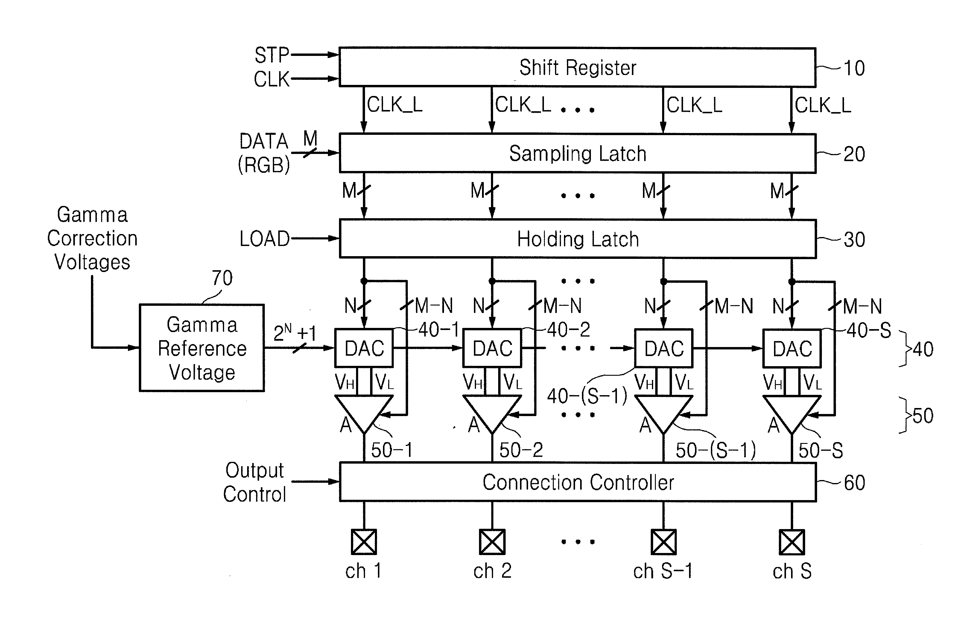
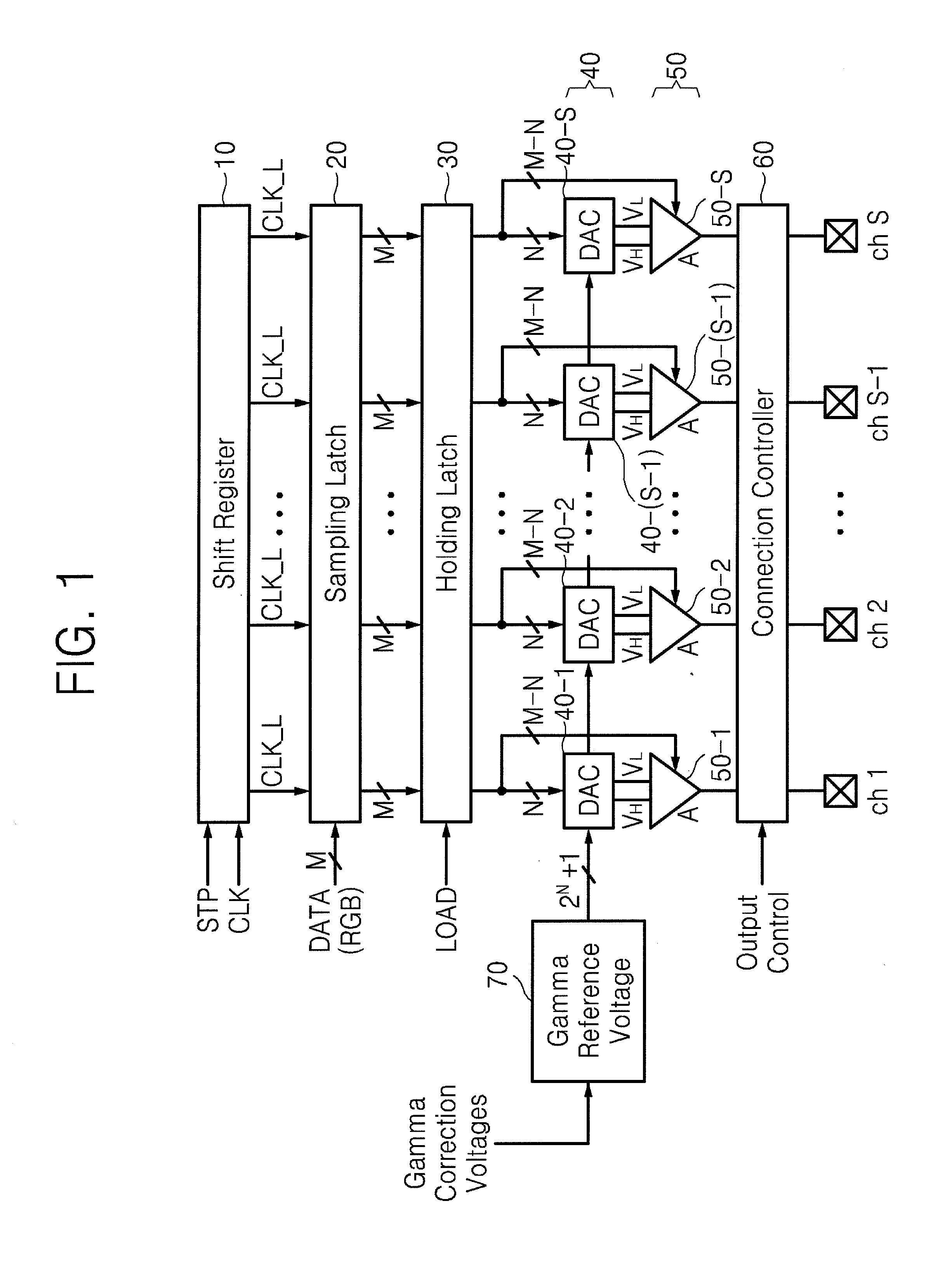
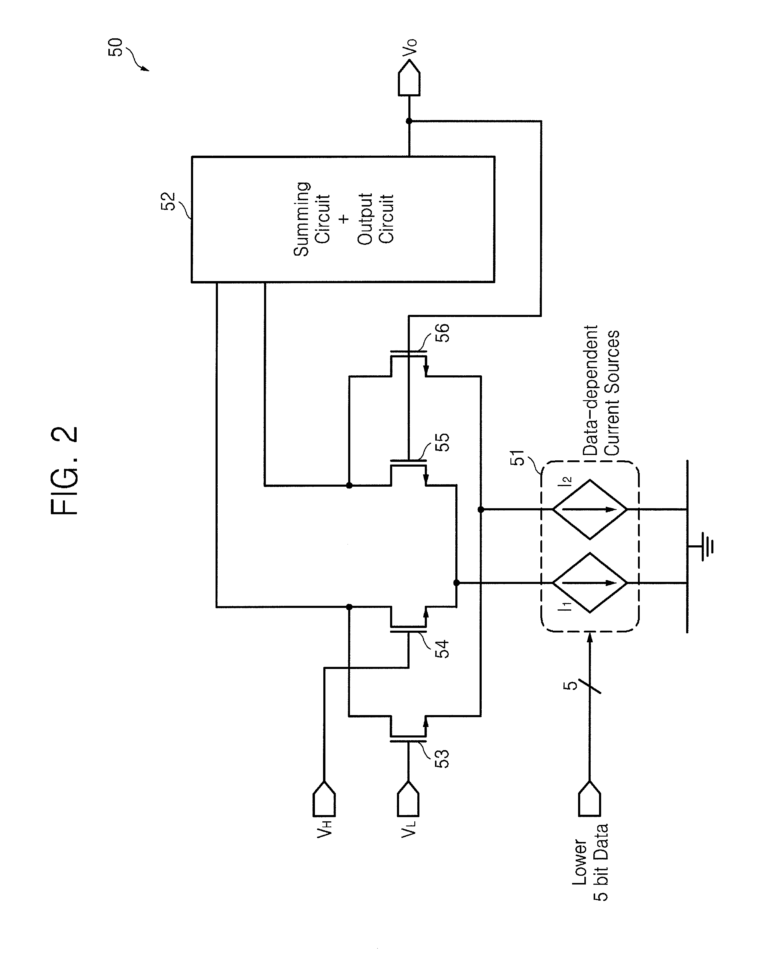
[0016]The buffer amplifier may include a first current digital-to-analog converter receiving the lower bits and outputting a first pair of bias currents in response to a first control signal, a current steering circuit receiving the first pair of bias currents, and a second current digital-to-analog converter receiving a second pair of bias currents from the current stee

Problems solved by technology

An increase in the area of the column driver IC typically correlates with an increase in production cost of the flat panel display.
However, a conventional buffer amplifier grows in size as the number of grays it is required to process increases.

Method used


Image

  • Digital-to-analog conversion circuit and column driver including the same
  • Digital-to-analog conversion circuit and column driver including the same
  • Digital-to-analog conversion circuit and column driver including the same

Examples


Embodiment Construction

[0024]The present invention now will be described more fully hereinafter with reference to the accompanying drawings, in which exemplary embodiments of the invention are shown. This invention may, however, be embodied in many different forms and should not be construed as limited to the exemplary embodiments set forth herein. In the drawings, the size and relative sizes of regions may be exaggerated for clarity. Like numbers refer to like elements throughout.

[0025]It will be understood that when an element is referred to as being “connected” or “coupled” to another element, it can be directly connected or coupled to the other element or intervening elements may be present.

[0026]A display panel may be driven by a display driver integrated circuit (IC). The display driver IC may include a column driver IC and a row driver IC. Rows of pixels included in the display panel may be sequentially selected by the row driver IC and a voltage or current corresponding to a gray level to be displ...


PUM


Abstract

A digital-to-analog conversion circuit includes a digital-to-analog converter and a buffer amplifier. The digital-to-analog converter receives upper bits of digital data and a plurality of analog voltages and is configured to output two adjacent analog voltages of the plurality of analog voltages based on the upper bits. The buffer amplifier includes two input terminals. One of the input terminals receives one of the two adjacent analog voltages and the other input terminal receives the other adjacent analog voltage. The buffer amplifier is configured to generate a current offset by controlling a current flowing into each of the two input terminals based on lower bits of the digital bits.

Description

CROSS-REFERENCE TO RELATED APPLICATIONS[0001]This application claims priority to Korean Patent Application No. 10-2008-0123253, filed on Dec. 5, 2008, in the Korean Intellectual Property Office (KIPO), the disclosure of which is incorporated by reference herein.BACKGROUND[0002]1. Technical Field[0003]Embodiments of the present invention relate to a signal conversion technique, and more particularly, to a digital-to-analog conversion circuit for controlling a bias current of an input terminal to minimize the area of a buffer amplifier, and to a column driver including the same.[0004]2. Discussion of Related Art[0005]The size of a digital-to-analog (DAC) conversion circuit of a flat panel display typically increases as the number of gray levels displayed by the flat panel display increases. The increase in size of the DAC circuit may cause an increase in the area of a column driver integrated circuit (IC). Further, increases in the resolution of a flat panel display for high definitio...

Claims


Application Information

Patent Timeline
IPC IPC(8): H03M1/00H03M1/66
CPCG09G3/20G09G2310/027G09G2310/0272H03M1/68H03M1/662H03M1/664G09G2310/0291H03M1/16H03M1/66
Inventor CHO, GYU HYEONGCHOI, YOON KYUNGKIM, HYOUNG RAEJEON, YONG JOONLEE, HYUNG MINLEE, SUNG WOO
Owner SAMSUNG ELECTRONICS CO LTD
Learn More