Page buffer circuit, nonvolatile device including the same, and method of operating the nonvolatile memory device

a buffer circuit and nonvolatile memory technology, applied in static storage, digital storage, instruments, etc., can solve the problems of narrowing the width of a distribution of threshold voltages, extending the program time of verification operations,

Active Publication Date: 2010-06-10
SK HYNIX INC
View PDF3 Cites 5 Cited by
  • Summary
  • Abstract
  • Description
  • Claims
  • Application Information

AI Technical Summary

Benefits of technology

[0017]One or more embodiments relate to a page buffer circuit, a nonvolatile memory device including the page buffer circuit, and a method of operating the nonvolatile memory device, wherein the program speeds of memory cells are classified into some groups by performing several verification operations in a similar way to a double verification operation upon a program operation, and the memory cells are programmed to have a narrow threshold voltage distribution by changing a program voltage based on the program speed of a corresponding memory cell on a group basis.

Problems solved by technology

However, the double verification operation may have an extended program time because a verification operation must be performed twice whenever a program operation is performed and has limitations in narrowing the width of a distribution of threshold voltages because of the repeated performance of the verification operations.

Method used


Image

  • Page buffer circuit, nonvolatile device including the same, and method of operating the nonvolatile memory device
  • Page buffer circuit, nonvolatile device including the same, and method of operating the nonvolatile memory device
  • Page buffer circuit, nonvolatile device including the same, and method of operating the nonvolatile memory device

Examples


Embodiment Construction

[0040]Hereinafter, some embodiments of the present disclosure will be described in detail with reference to accompanying drawings. The drawing figures are provided to allow those having ordinary skill in the art to understand the scope of the embodiment of the disclosure.

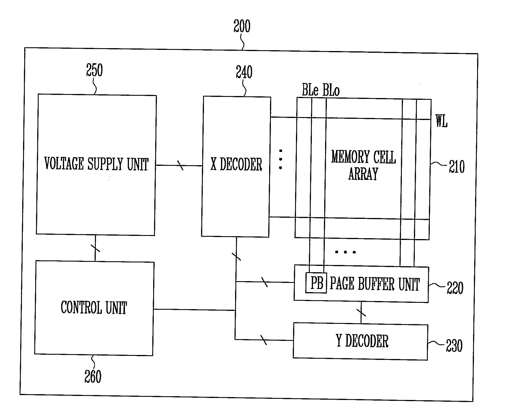
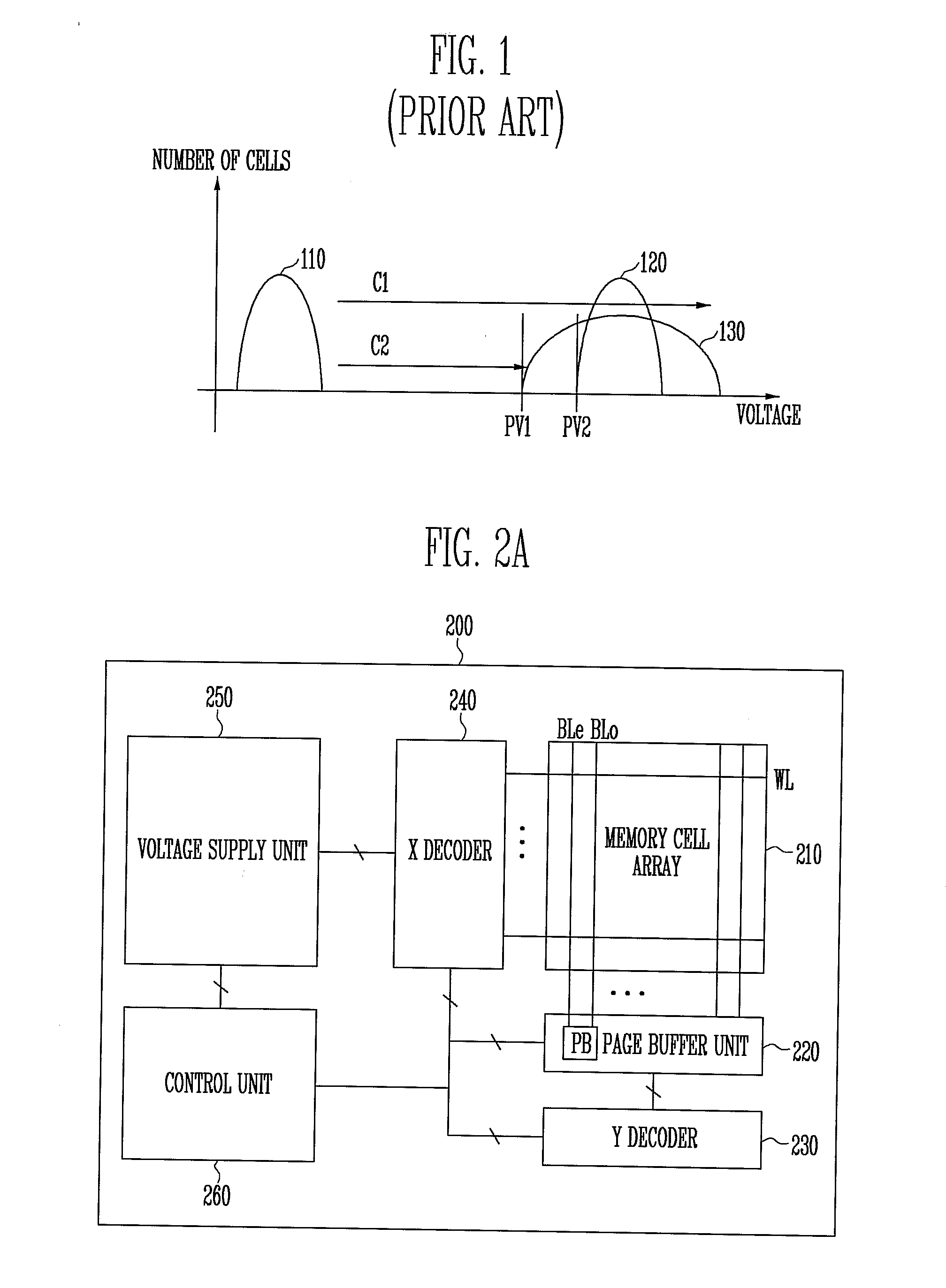
[0041]FIG. 2A is a block diagram of a nonvolatile memory device according to some embodiments.

[0042]Referring to FIG. 2A, a nonvolatile memory device 200 according to the present embodiment includes a memory cell array 210, a page buffer unit 220, a Y decoder 230, an X decoder 240, a voltage supply unit 250, and a control unit 260.

[0043]The memory cell array 210 includes memory blocks each including memory cells for storing data. The memory cells are connected to each other by word lines and bit lines.

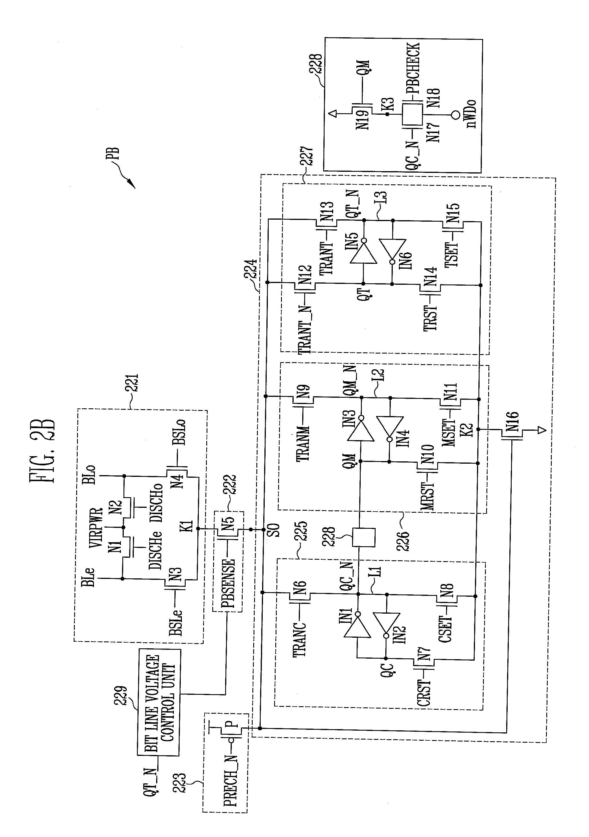
[0044]The page buffer unit 220 includes page buffers PB coupled to the bit lines. The page buffer PB is coupled to the memory cell through the bit lines configured to store data to be programmed into a memory cell or r...


PUM


Abstract

A page buffer circuit comprises a sense unit, a latch unit, and a bit line voltage control unit. The sense unit is configured to couple a bit line and a sense node in response to a sense control signal in response to the sense control signal. The latch unit includes a plurality of latch circuits configured to latch data programmed or to be programmed. The bit line voltage control unit is configured to classify program states of memory cells, coupled to the selected bit line, into first to nth groups by performing first to nth verification operations after a first program operation of a program operation and is configured to control a voltage level of the sense control signal in order to transfer a bit line voltage to the selected bit line.

Description

CROSS-REFERENCE TO RELATED APPLICATION[0001]Priority to Korean patent application number 10-2008-0123869 filed on Dec. 8, 2008, the entire disclosure of which is incorporated by reference herein, is claimed.BACKGROUND[0002]An embodiment relates to a page buffer circuit of a nonvolatile memory device and a program operation and, more particularly, to a page buffer circuit, a nonvolatile memory device including the page buffer circuit, and a method of operating the nonvolatile memory device, wherein the program speeds of memory cells are classified into some groups and the program speeds of the memory cells are controlled on a group basis so that the memory cells have a threshold voltage distribution with a narrow width thereof.[0003]A NAND flash memory device (i.e., a type of a nonvolatile memory device) includes a memory cell array, a row decoder, and a page buffer. The memory cell array includes word lines extending in rows, bit lines extending in columns, and cell strings correspo...

Claims


Application Information

Patent Timeline
Patent Type & Authority Applications(United States)
IPC IPC(8): G11C16/04G11C16/06G11C7/10
CPCG11C7/1039G11C7/12G11C11/5628G11C2216/14G11C16/3454G11C2211/5621G11C16/26G11C16/06G11C16/24G11C16/34
Inventor RHO, JUN RYEKOO, CHEUL HEE
Owner SK HYNIX INC
Why Eureka
Try Eureka