
Semiconductor memory device and programming method thereof

Active Publication Date: 2015-03-12
SK HYNIX INC
View PDF2 Cites 17 Cited by
  • Summary
  • Abstract
  • Description
  • Claims
  • Application Information

AI Technical Summary

Benefits of technology

This patent is about a type of semiconductor memory that has a way to make sure it's always running at the best possible speed and efficiency. This helps to make sure that data is always being stored and accessed quickly and correctly.

Problems solved by technology

A volatile memory device is unable to retain its stored data when the power is turned off.
However, with the increased degree of integration of the semiconductor memory device, problems have arisen in the operations of the semiconductor memory device, such as coupling between neighboring cells, a wider threshold voltage distribution width resulting from a program disturb, or increased programming time to reduce the threshold voltage distribution width.

Method used


Image

  • Semiconductor memory device and programming method thereof
  • Semiconductor memory device and programming method thereof
  • Semiconductor memory device and programming method thereof

Examples


Embodiment Construction

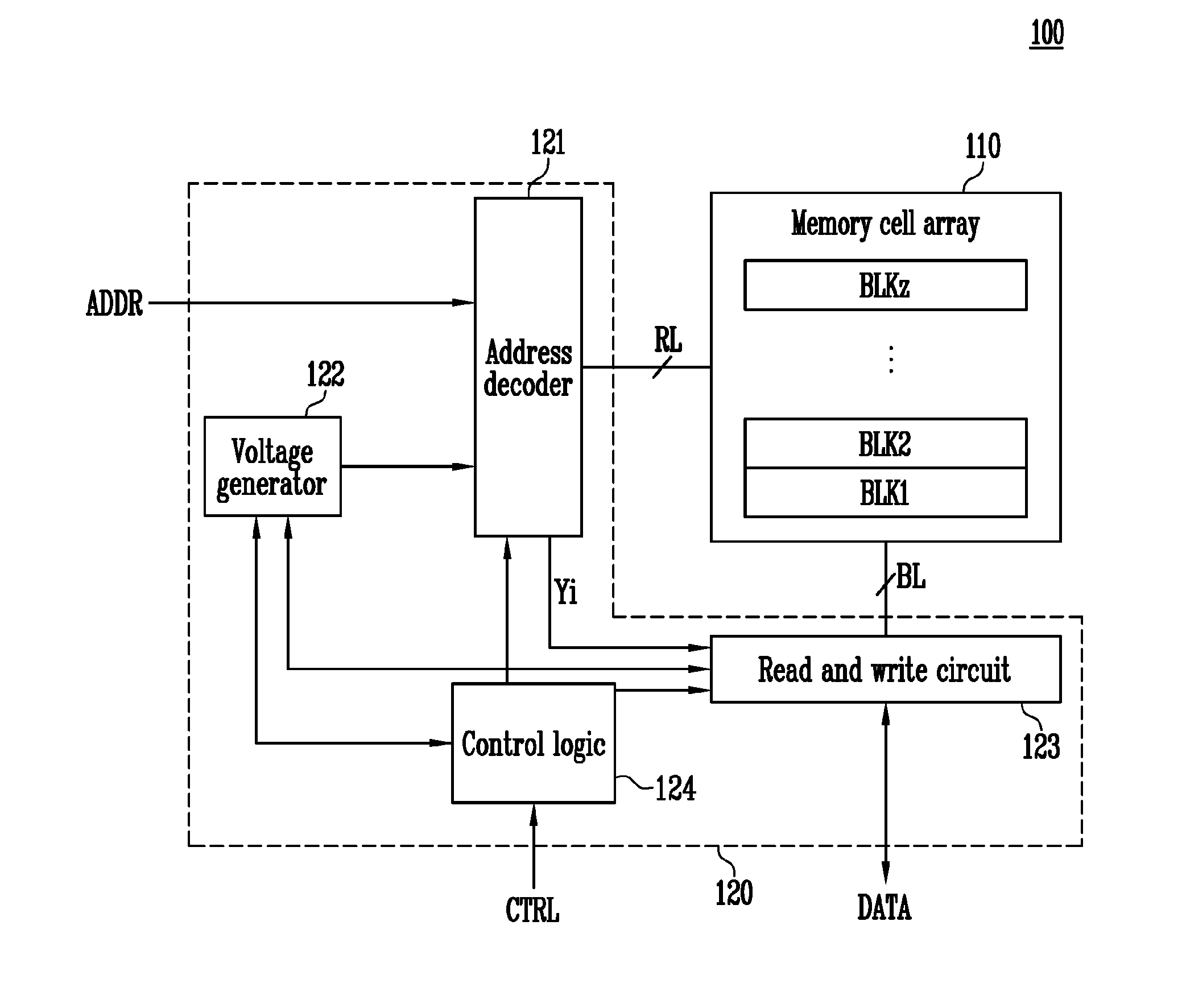
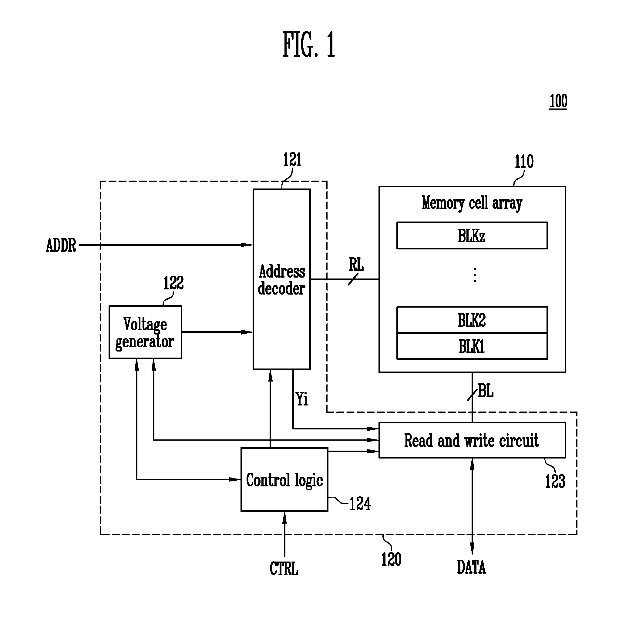
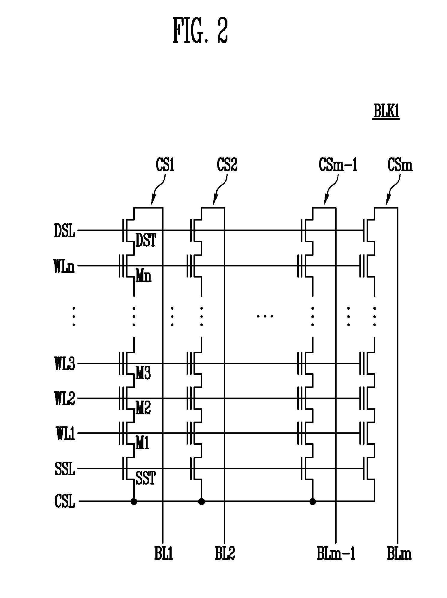
[0026]Hereinafter, various embodiments will be described in detail with reference to the accompanying drawings. The figures are provided to allow those having ordinary skill in the art to understand the scope of the embodiments of the disclosure. The present invention may, however, be embodied in different forms and should not be construed as limited to the embodiments set forth herein. Rather, these embodiments are provided so that this disclosure will be thorough and complete, and will fully convey the scope of the present invention to those skilled in the art.

[0027]Furthermore, ‘connected / coupled’ represents that one component is directly coupled to another component or indirectly coupled through another component. In this specification, a singular form may include a plural form as long as it is not specifically mentioned in a sentence. Furthermore, ‘include / comprise’ or ‘including / comprising’ used in the specification represents that one or more components, steps, operations, an...


PUM


Abstract

A programming method of a semiconductor memory device includes, in an n-th program loop, applying a first program pulse to a first memory cell group, applying a second program pulse to a second memory cell group, and determining first fast cells and first slow cells in the first memory cell group, and in an n+1-th program loop, applying a third program pulse, which is increased by a step voltage from the first program pulse, to the first fast cells in the first memory cell group, and applying a fourth program pulse, which is increased by the step voltage from the second program pulse, to the first slow cells in the first memory cell group and the second memory cell group.

Description

CROSS-REFERENCE TO RELATED APPLICATION[0001]The present application claims priority to Korean patent application number 10-2013-0108572 filed on Sep. 10, 2013, in the Korean Intellectual Property Office, the entire disclosure of which is incorporated by reference herein.BACKGROUND[0002]1. Technical Field[0003]Various embodiments relate generally to a semiconductor memory device and a programming method thereof.[0004]2. Related Art[0005]A semiconductor memory device is a storage device that is realized using a semiconductor made from, for example, silicon (Si), germanium (Ge), gallium arsenide (GaAs), or indium phosphide (InP). Semiconductor memory devices can be classified as volatile memory devices or nonvolatile memory devices.[0006]A volatile memory device is unable to retain its stored data when the power is turned off. The volatile memory device includes a static random access memory (SRAM) device, a dynamic RAM (DRAM) device, a synchronous DRAM (SDRAM) device, or the like. A n...

Claims


Application Information

Patent Timeline
IPC IPC(8): G11C16/12G11C16/34
CPCG11C16/3459G11C16/12G11C11/5628G11C16/0483G11C16/3404G11C16/10
Inventor KIM, NAM HOONLEE, MIN KYU
Owner SK HYNIX INC
Learn More