Method for Stacking Semiconductor Dies

a technology of semiconductor dies and stacking, which is applied in the direction of semiconductor devices, basic electric elements, electrical appliances, etc., can solve the problems of method failure, material fragility, and inability to withstand the stress of various process steps very well, so as to reduce or eliminate potential damage, improve the yield of dies, and handle stress better

Inactive Publication Date: 2010-06-10
TAIWAN SEMICON MFG CO LTD
View PDF8 Cites 36 Cited by
  • Summary
  • Abstract
  • Description
  • Claims
  • Application Information

AI Technical Summary

Benefits of technology

[0008]In accordance with yet another preferred embodiment of the present invention, a method for forming semiconductor devices comprises providing a semiconductor wafer having an inner die area surrounded by a scriber line and an outer area immediately adjacent to the scribe line, the semiconductor wafer comprising a first side and a second side. Conductive vias are formed partially through the semiconductor wafer from the first side, and the inner die area on the second side of the wafer is thinned to expose the conductive vias without thinning the outer area.
[0009]An advantage of a preferred embodiment of the present invention is that the unthinned portion of the wafer allows the wafer to better handle stresses that are inherent in later processing steps and handling of the wafer. This ability reduces or eliminates potential damage that could occur through processing and handling, thereby leading to an increased yield of dies.

Problems solved by technology

However, as materials such as low-k or extremely low-k dielectrics are beginning to become more widely used, these methods become a problem.
These materials are very fragile and do not withstand the stresses from various process steps very well.
This problem becomes magnified when the wafers are thinned by mechanical grinding or etching as the dielectrics may become unable to stand further handling and processing, which may result in damage and, eventually, device failure.

Method used


Image

  • Method for Stacking Semiconductor Dies
  • Method for Stacking Semiconductor Dies
  • Method for Stacking Semiconductor Dies

Examples


Embodiment Construction

[0017]The making and using of the presently preferred embodiments are discussed in detail below. It should be appreciated, however, that the present invention provides many applicable inventive concepts that can be embodied in a wide variety of specific contexts. The specific embodiments discussed are merely illustrative of specific ways to make and use the invention, and do not limit the scope of the invention.

[0018]The present invention will be described with respect to preferred embodiments in a specific context, namely stacked dies utilizing through-silicon vias in a semiconductor wafer. The invention may also be applied, however, to other thin wafer handling processes.

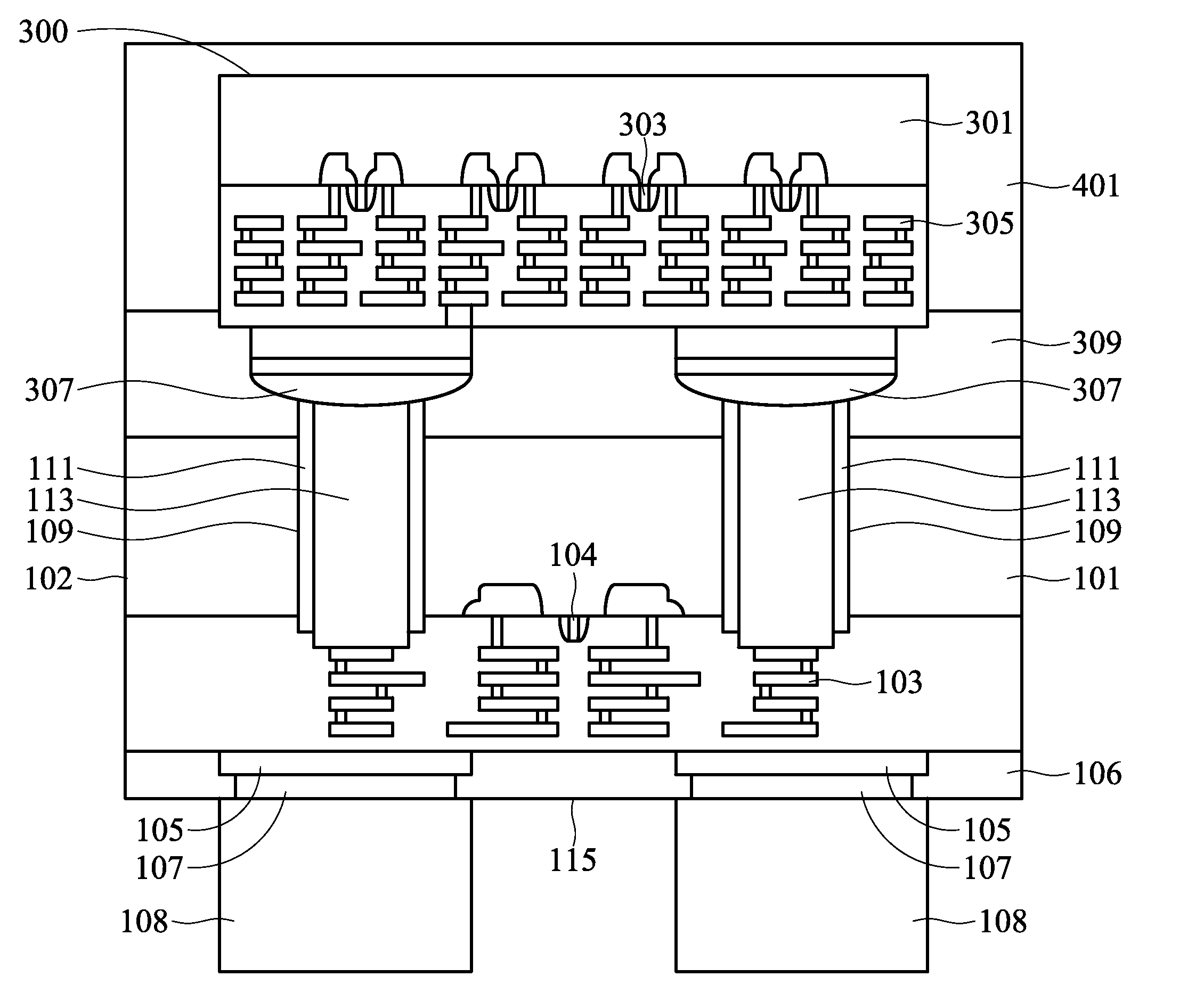
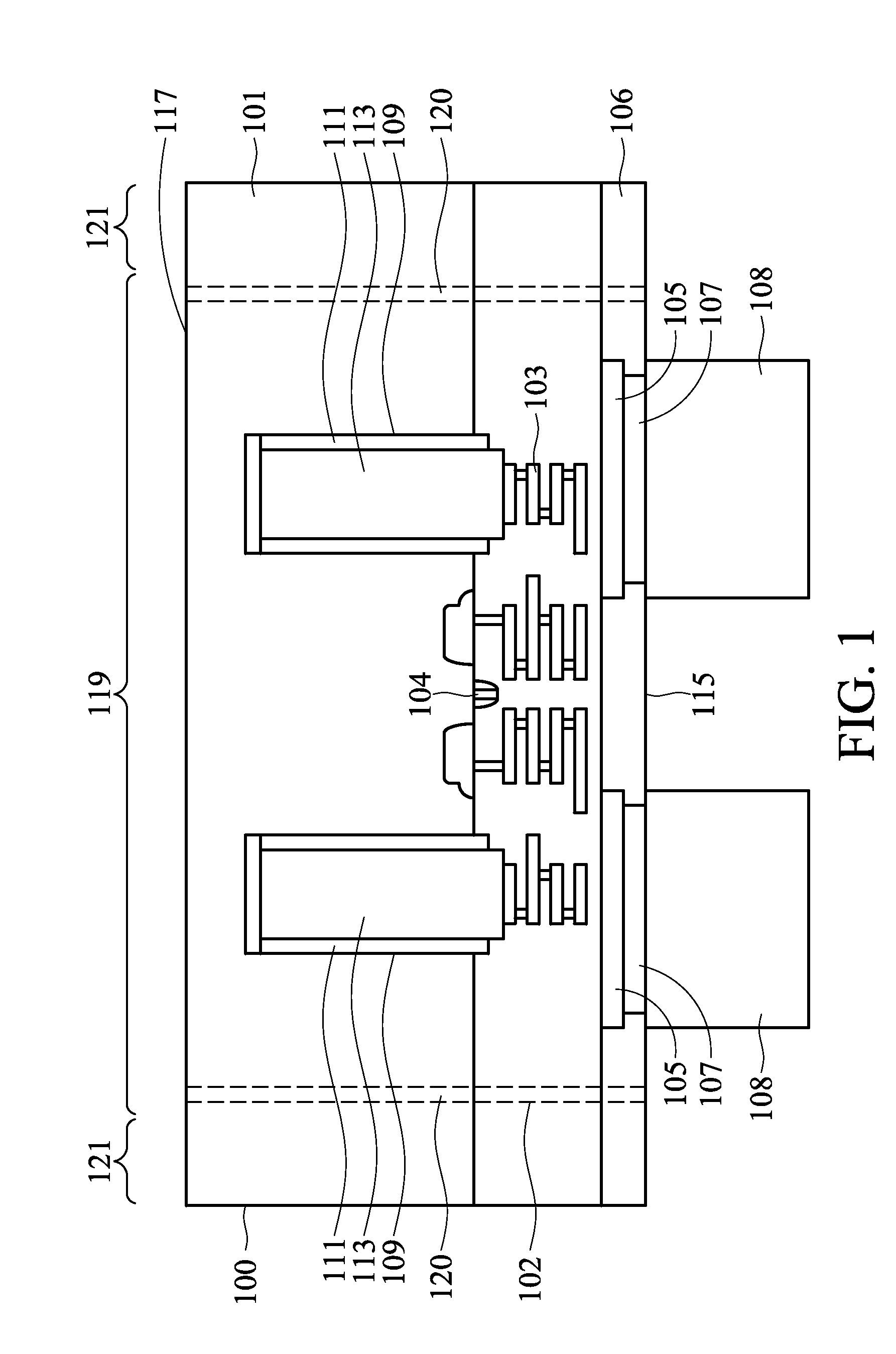
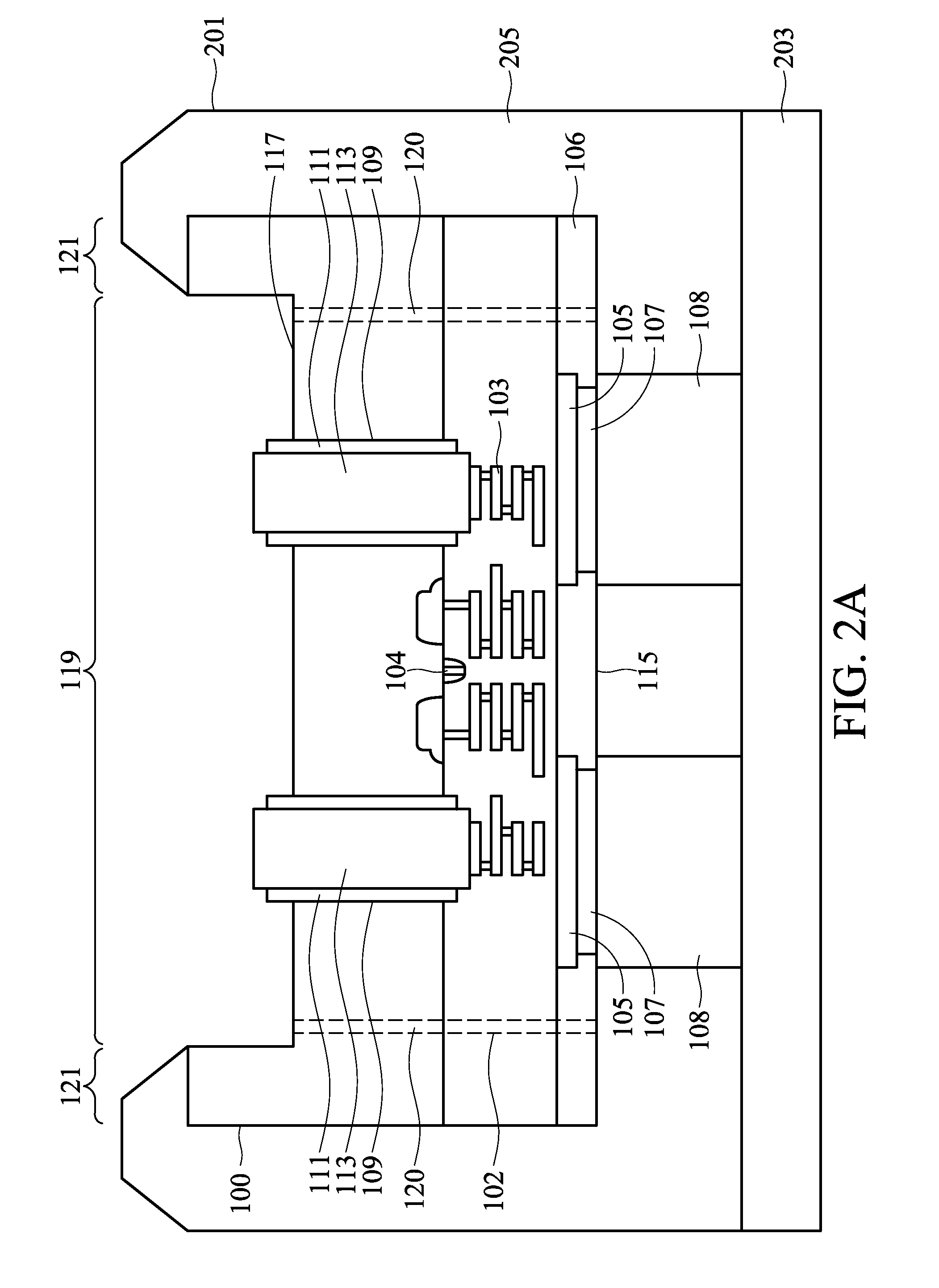
[0019]With reference now to FIG. 1, there is shown a cross-sectional view of a wafer 100 with a front side 115 and a backside 117. The wafer 100 preferably has a plurality of first semiconductor dies 102 (outlined by the dashed lines) formed in a die area 119 of the wafer 100, a scribe line 120 adjacent to the die...


PUM


Abstract

A system and method for stacking semiconductor dies is disclosed. A preferred embodiment comprises forming through-silicon vias through the wafer, protecting a rim edge of the wafer, and then removing the unprotected portions so that the rim edge has a greater thickness than the thinned wafer. This thickness helps the fragile wafer survive further transport and process steps. The rim edge is then preferably removed during singulation of the individual dies from the wafer.

Description

TECHNICAL FIELD[0001]The present invention relates generally to a system and method for connecting semiconductor dies and, more particularly, to a system and method for connecting semiconductor dies utilizing a through-silicon via.BACKGROUND[0002]Generally, two semiconductor dies may be connected using through-silicon vias (TSVs), which generally require some type of removal of material from the backside of the wafers on which the semiconductor dies are formed. In one method of forming TSVs, a portion of the side of the wafer containing active devices is removed to form one or more holes at least part of the way through the silicon wafer. After the holes have been filled with a conductive material, the backside of the wafer is removed using a process such as mechanical grinding or etching in order to expose the conductive material and form a contact through the backside of the wafer to the front side of the wafer.[0003]However, as materials such as low-k or extremely low-k dielectri...

Claims


Application Information

Patent Timeline
Patent Type & Authority Applications(United States)
IPC IPC(8): H01L21/46H01L21/465
CPCH01L21/76898H01L25/0657H01L25/50H01L21/486H01L2225/06513H01L2225/06541H01L2924/01019H01L2224/73203H01L2224/0401H01L2224/13009H01L2224/13111H01L2224/13139H01L2224/13147H01L2224/14181H01L2224/16146H01L2224/32145H01L2224/73204H01L2224/94H01L2224/11H01L2224/16145H01L2924/00
Inventor YANG, KU-FENGWU, WENG-JINCHIOU, WEN-CHIHYU, CHEN-HUA
Owner TAIWAN SEMICON MFG CO LTD
Why Eureka
Try Eureka