Reading method of nonvolatile semiconductor memory device

a nonvolatile, memory device technology, applied in static storage, digital storage, instruments, etc., can solve the problems of difficult to secure margin, difficult to secure sufficient margin, reading error, etc., to accelerate the start-up time of word line voltage and improve the reading accuracy of high-speed read operation.

Active Publication Date: 2010-06-17
SAMSUNG ELECTRONICS CO LTD
View PDF5 Cites 9 Cited by
  • Summary
  • Abstract
  • Description
  • Claims
  • Application Information

AI Technical Summary

Benefits of technology

[0009]It is therefore a feature of an embodiment to provide a reading method of a nonvolatile memory device that is adapted to accelerate a start-up time of a word line voltage as compared to conventional reading methods.
[0

Problems solved by technology

This leads to reading error and difficulty in securing margin.
Furthermore, it is difficult to secure sufficient margin because a load of a word line becomes heavier with increased capacitance

Method used


Image

  • Reading method of nonvolatile semiconductor memory device
  • Reading method of nonvolatile semiconductor memory device
  • Reading method of nonvolatile semiconductor memory device

Examples


Embodiment Construction

[0038]Japanese Patent Application No. 2008-315854, filed on Dec. 11, 2008, in the Japanese Intellectual Property Office, and Korean Patent Application No. 10-2009-0074848, filed on Aug. 13, 2009, in the Korean Intellectual Property Office, are incorporated by reference herein in their entirety.

[0039]Exemplary embodiments will now be described more fully hereinafter with reference to the accompanying drawings; however, they may be embodied in different forms and should not be construed as limited to the embodiments set forth herein. Rather, these embodiments are provided so that this disclosure will be thorough and complete, and will fully convey the scope of the invention to those skilled in the art. Like reference numerals refer to like elements / features throughout the specification.

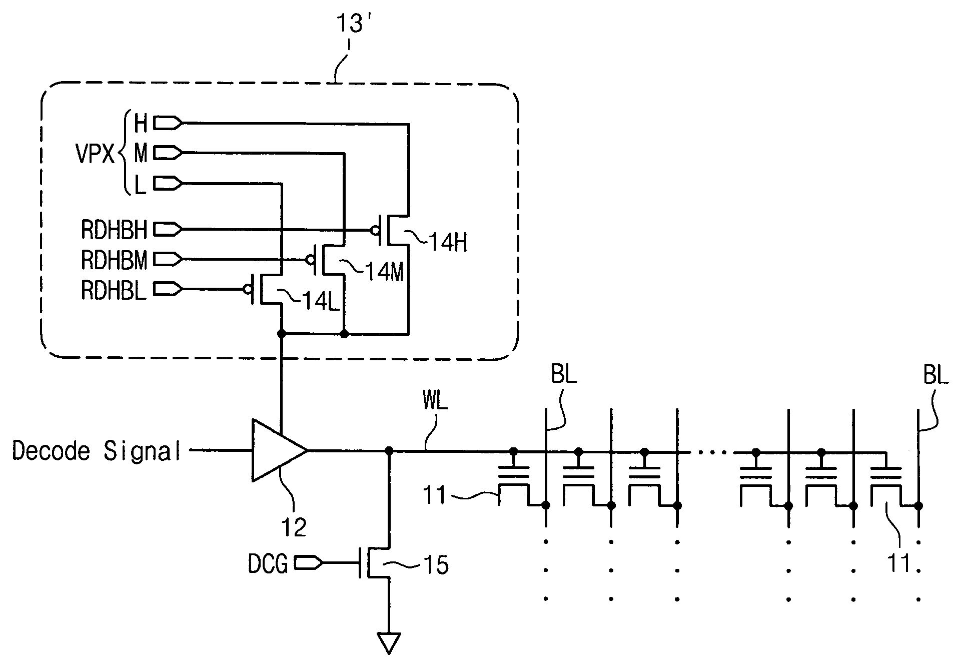
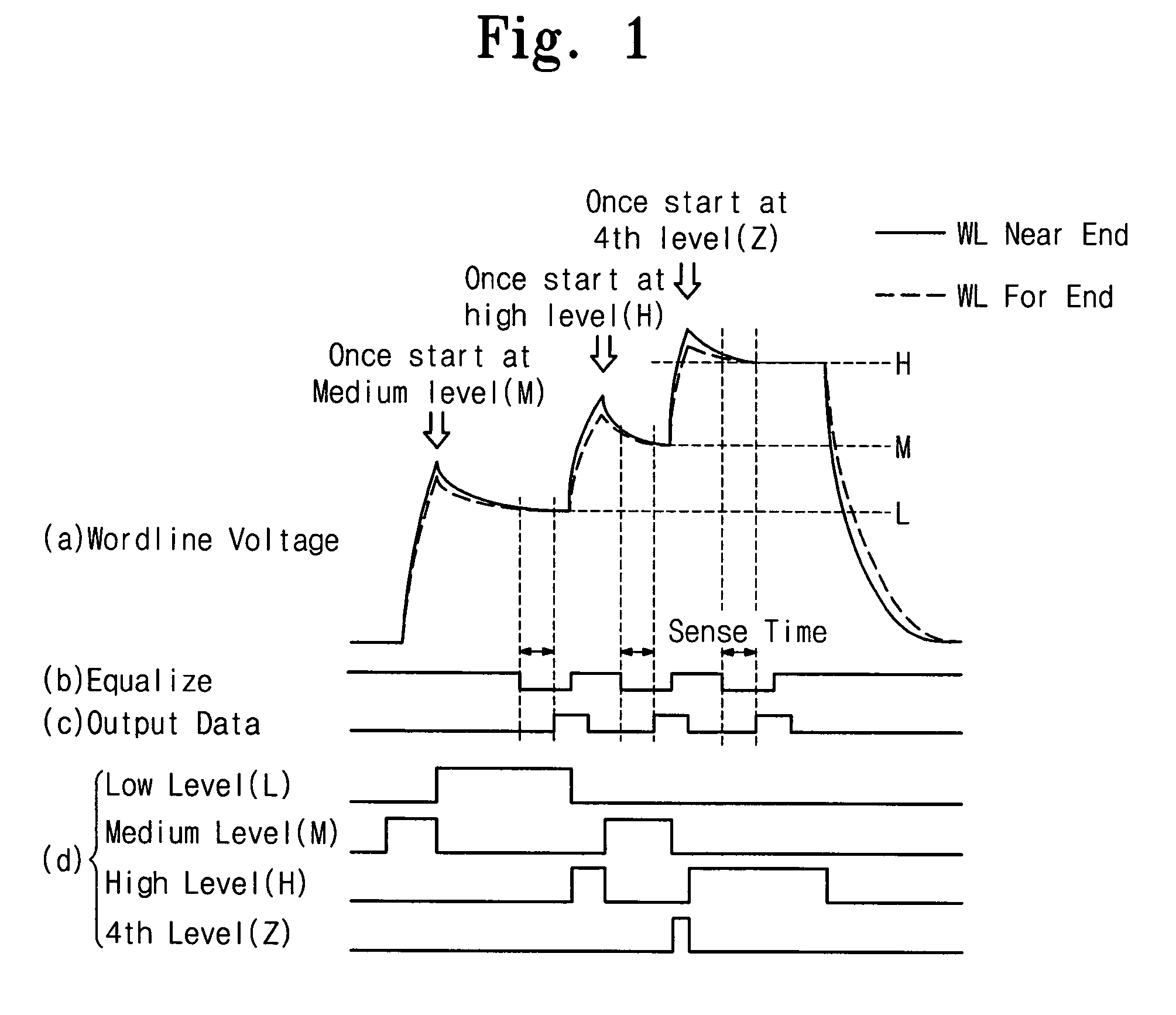
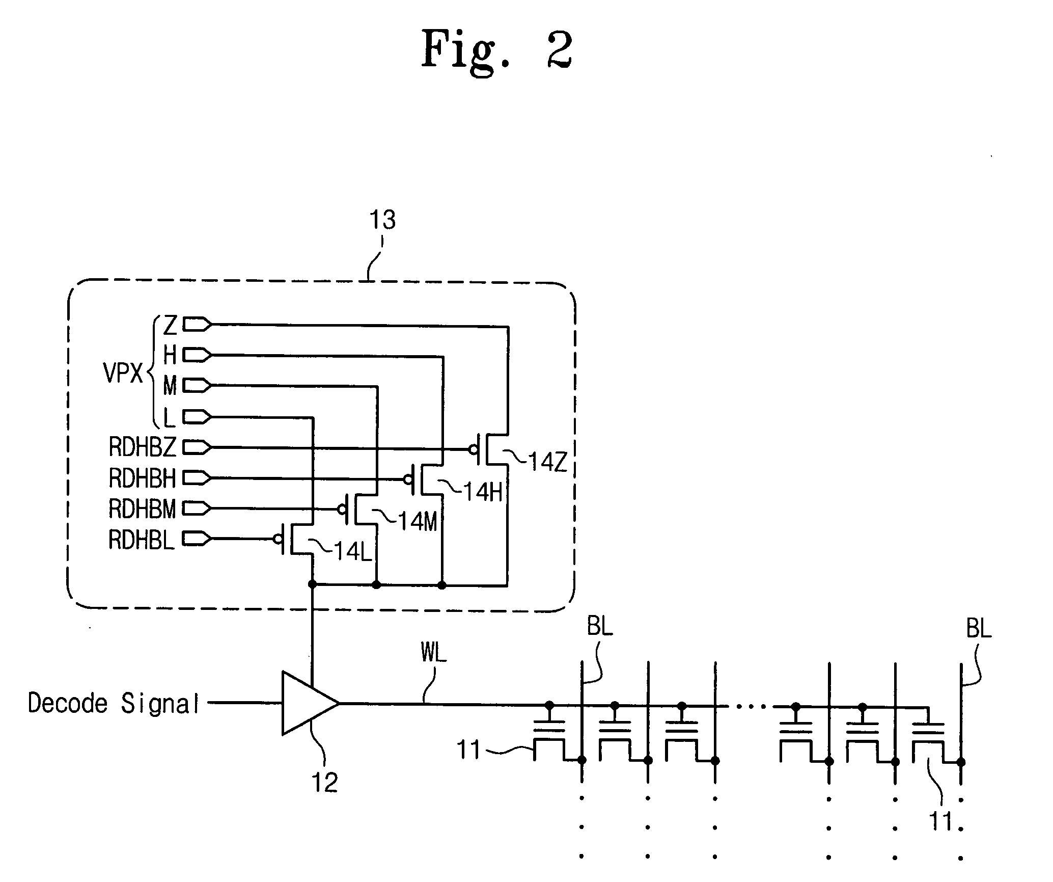
[0040]A reading method according to the exemplary embodiment may be applied to a multi-level cell (MLC) nonvolatile memory device in which a read operation may be performed by supplying a low-level (L) ...


PUM


Abstract

Reading methods of a nonvolatile semiconductor memory device are described herein. Methods may include supplying, to a word line, one of a voltage corresponding to a highest reading level or a voltage having a level higher than a first reading level of a read operation to be performed on the word line, and subsequently supplying a voltage of the first reading level to the word line and performing the read operation.

Description

BACKGROUND[0001]1. Field[0002]Embodiments relate to nonvolatile semiconductor memory devices, including non-volatile memory devices having a multi-level cell architecture. More particularly, embodiments relate to a reading method of a nonvolatile memory device that may be effectively applied to non-volatile memory devices that have a multi-level cell architecture.[0003]2. Description of the Related Art[0004]A multi-level cell (MLC) architecture is useful in storing multi-data in nonvolatile semiconductor memory devices. In nonvolatile semiconductor memory devices employing the MLC architecture, N−1 word line voltage supplying steps are required for a one-time read operation. Here, N is a number representing a critical value in an MLC, and N−1 corresponds to 3 normally.[0005]In general, in an MLC device, a word line voltage may be controlled through three steps, i.e., low-level (L) step, medium-level (M) step, and high-level (H) step. Further, during a read operation in an MLC nonvol...

Claims


Application Information

Patent Timeline
IPC IPC(8): G11C16/04
CPCG11C16/26G11C11/5642
Inventor TANAKA, TSUYOSHI
Owner SAMSUNG ELECTRONICS CO LTD
Why Eureka
Try Eureka